

Mesa-type bipolar transistor
a bipolar transistor, a technology of asymmetric transistors, applied in the direction of diodes, semiconductor devices, electrical apparatus, etc., can solve the problems of not being defined, maintaining the appropriate current gain, and reducing the transistor size at the same time, and achieve excellent repeatability and high controllability
- Summary
- Abstract
- Description
- Claims
- Application Information
AI Technical Summary
Benefits of technology
Problems solved by technology
Method used
Image

Examples
first embodiment
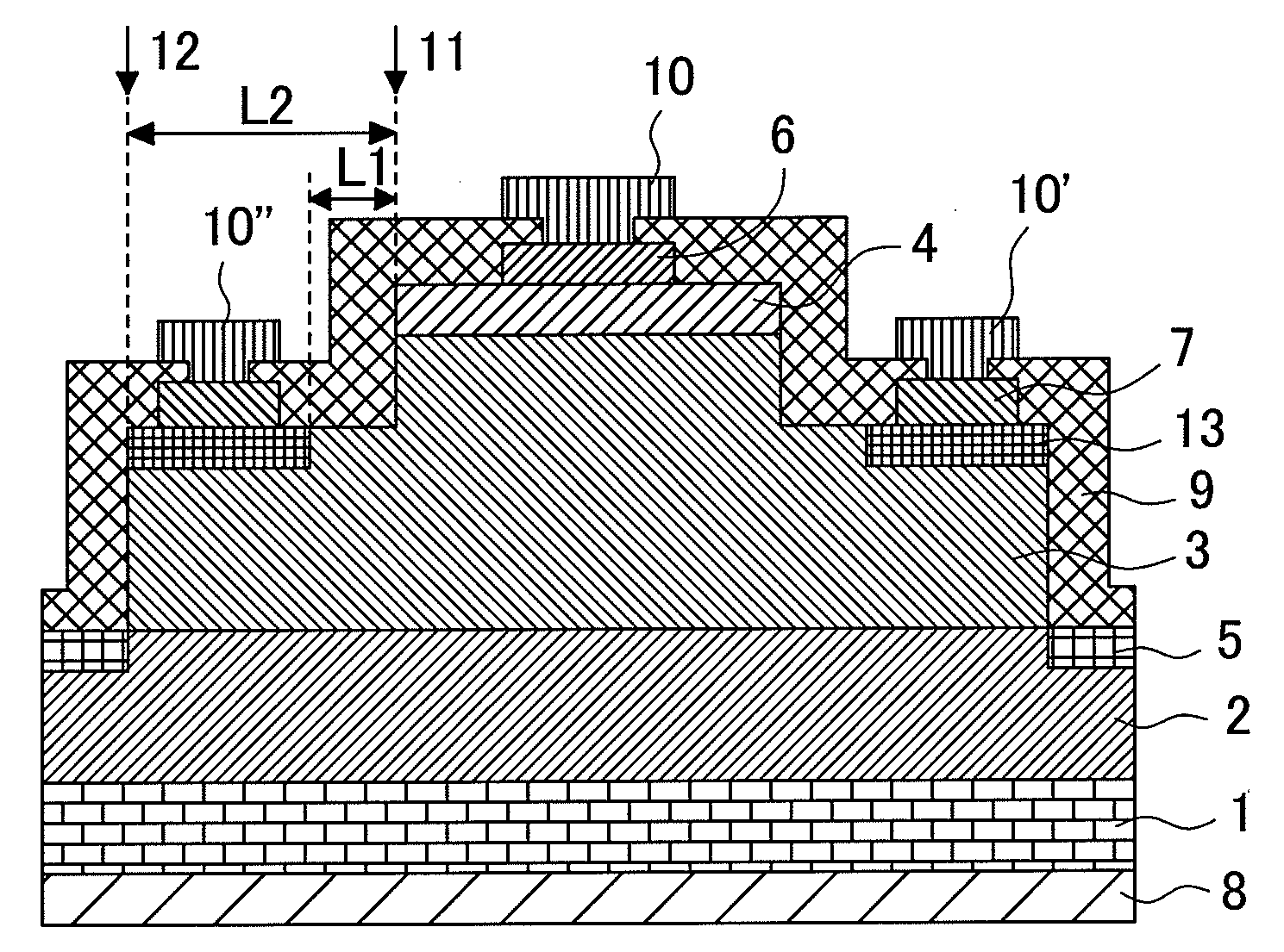
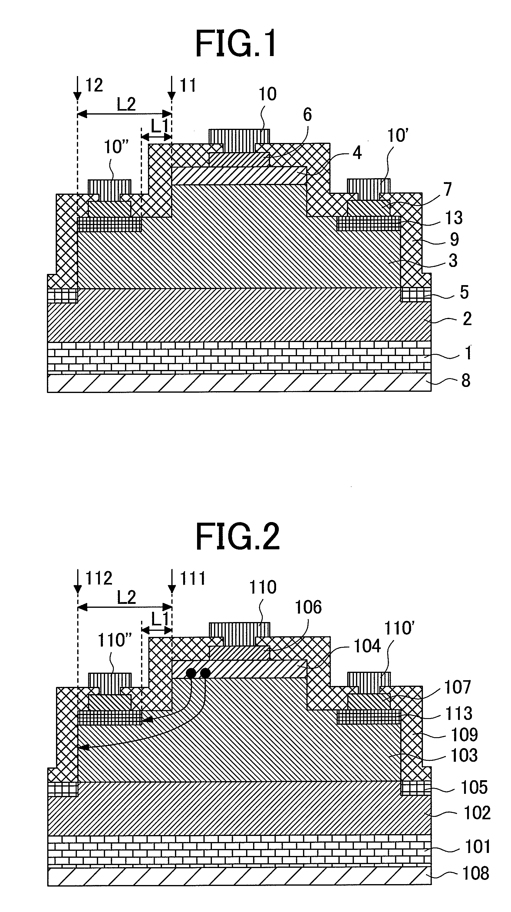
[0047]An npn-type SiC bipolar transistor according to a first embodiment of the present invention, and an associated manufacturing process are described below using FIGS. 1, 5, 7 to 13.
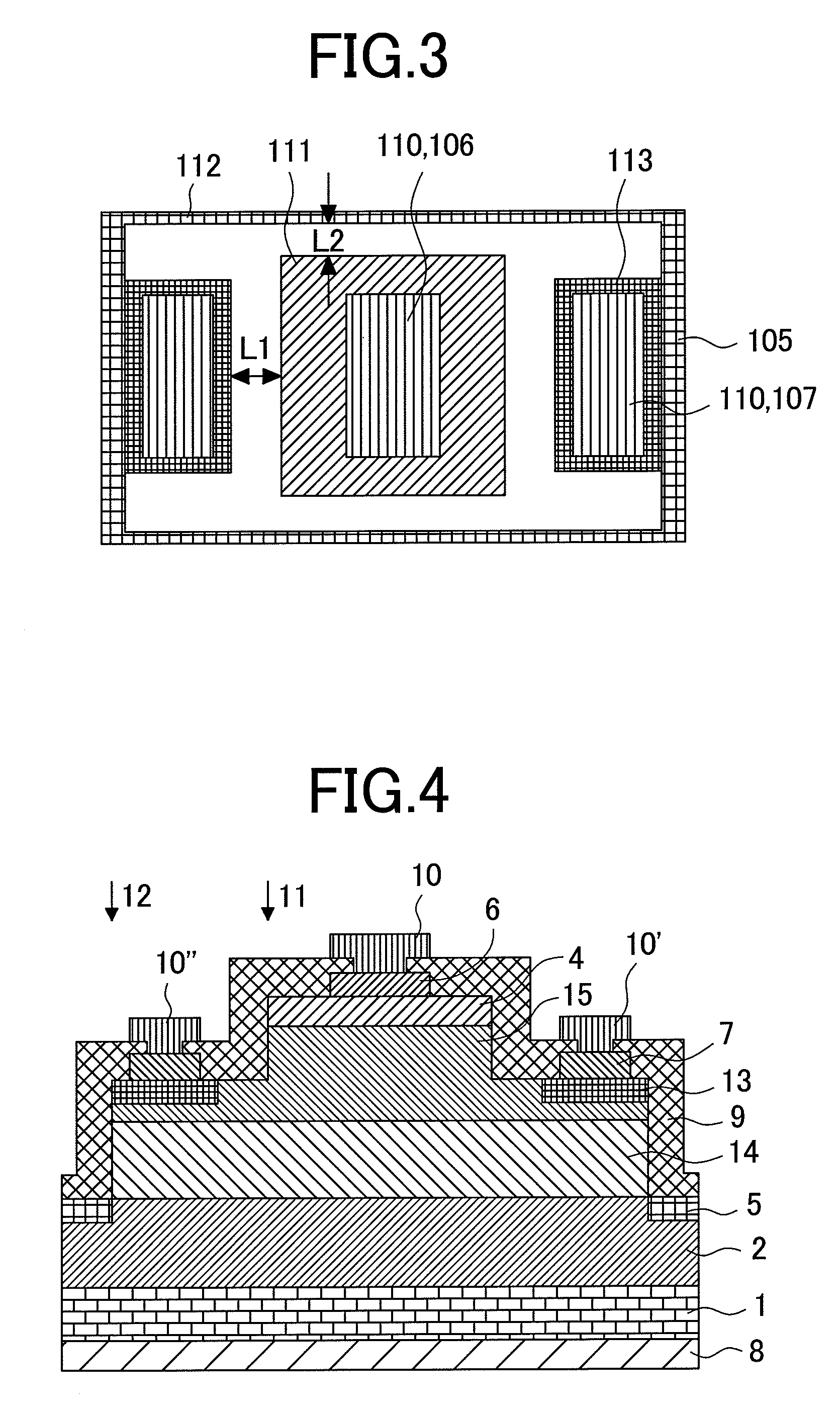
[0048]FIG. 1 is a longitudinal sectional structural view of this npn-type SiC bipolar transistor according to the first embodiment of the present invention. FIG. 13 is a plan view of this transistor. In both figures, reference numbers and symbols are used similarly. A collector layer 2 made of n-type SiC with a thickness of 15 μm and a donor (N) density of 2×1016 cm−3, a base layer 3 made of p-type SiC with a thickness of 1 μm, and an emitter layer 4 made of n-type SiC with a thickness of 1 μm and a donor (N) density of 3×1019 cm−3 are formed on an n-type SiC substrate 1 having a (0001) Si surface and a donor (N) density of 3×1018 cm−3. Also, the emitter layer 4 and the base layer 3 form a mesa structure 11. In addition, ohmic electrodes are formed as follows: a nickel / titanium (Ni / Ti) alloyed emitter...
second embodiment
[0060]Another npn-type SiC bipolar transistor according to a second embodiment of the present invention, and an associated manufacturing process are described below using FIGS. 1, 5, and 13.
[0061]A longitudinal sectional structural view of the npn-type SiC bipolar transistor according to the second embodiment of the present invention, is essentially the same as in FIG. 1. FIG. 13 is a plan view of the transistor. A collector layer 2 made of n-type SiC with a thickness of 15 μm and a donor (N) density of 2×1016 cm−3, a base layer 3 made of p-type SiC with a thickness of 1 μm, and an emitter layer 4 made of n-type SiC with a thickness of 1 μm and a donor (N) density of 3×1019 cm−3 are present on an n-type SiC substrate 1 having a (0001) Si surface and a donor (N) density of 3×1018 cm3. Also, the emitter layer 4 and the base layer 3 form a mesa structure 11, and the base layer 4 and the collector layer 2 form a second mesa structure 12. In addition, ohmic electrodes are formed as follo...
third embodiment
[0067]An npn-type GaN bipolar transistor according to a third embodiment of the present invention, and an associated manufacturing process are described below using FIGS. 1, 5, and 10 to 13.
[0068]A longitudinal sectional structural view of this npn-type GaN bipolar transistor according to the third embodiment of the present invention is essentially the same as in FIG. 1. FIG. 13 is a plan view of the transistor. A collector layer 2 made of n-type GaN with a thickness of 15 μm and a donor (Si) density of 2×1016 cm−3, a base layer 3 made of p-type GaN with a thickness of 1 μm, and an emitter layer 4 made of n-type GaN with a thickness of 1 μm and a donor (Si) density of 3×1019 cm−3 are present on an n-type GaN substrate 1 having a (0001) Ga surface and a donor (Si) density of 3×1018 cm−3. Also, the emitter layer 4 and the base layer 3 form a mesa structure 11. In addition, ohmic electrodes are formed as follows: a Ti / Al alloyed emitter electrode 6 is formed directly on the emitter lay...
PUM
 Abstract
Description
Claims
Application Information