Semiconductor memory device

a memory device and semiconductor technology, applied in the field of semiconductor memory devices, can solve the problems of reducing the size of the column of sense amplifiers, affecting the performance, and the influence of noise is more serious, so as to improve the charge transferring speed of the hierarchical switch, suppress the noise of bit lines, and increase the operation margin of the semiconductor memory device.

Active Publication Date: 2007-10-18
PANASONIC SEMICON SOLUTIONS CO LTD
View PDF14 Cites 14 Cited by
  • Summary
  • Abstract
  • Description
  • Claims
  • Application Information

AI Technical Summary

Benefits of technology

[0073]Thus, during the period of the charge sharing and during the amplification performed by the sense amplifier, a voltage between the gate and the source of the hierarchical switch can be increased, so as to improve the charge transferring speed of the hierarchical switch.
[0074]According to the present invention, in a semiconductor memory device having the hierarchical bit line architecture, the timing for operating the hierarchical switch is controlled for suppressing bit line noise. Accordingly, the operation margin of the semiconductor memory device can be increased.

Problems solved by technology

On the other hand, the size reduction of a column of sense amplifiers has not been proceeded as much as that of memory cell transistors.
This is for the following reason: Although a sense amplifier is required to accurately amplify a small signal read from a memory, when the size of transistors included in the sense amplifier is reduced, the electric characteristics are varied among the transistors, resulting in degrading the performance.
First, in turning off the hierarchical switches of the blocks not accessed at the time tb, coupling derived from a gate-source capacitance of a transistor included in each hierarchical switch causes common mode noise for lowering a bit line precharge level. This is noise peculiar to the hierarchical bit line architecture. In the hierarchical bit line architecture including four local bit lines per global bit line as shown in FIG. 16, three hierarchical switch transistors cause the coupling noise. The influence of this noise is more serious as the number of local bit lines is increased.
Secondly, noise from adjacent bit lines derived from side coupling capacitance with adjacent bit lines is caused during a period of the charge sharing when the data is read out to one of the bit lines from the memory capacitor with the word line activated at the time tc and during the amplification performed by the sense amplifier after the time td. In the hierarchical bit line architecture, the ratio of the side coupling capacitance to total bit line capacitance is larger than in the non-hierarchical bit line architecture.
As a result, the hierarchical bit line architecture is easily affected by the noise from adjacent bit lines.
(If any hierarchical switch is disposed against the periodicity of the arrangement, it is necessary to provide a dummy cell on a boundary between a memory cell and the hierarchical switch, and area overhead cannot be avoided.)
Therefore, it is difficult to use such a transistor as a hierarchical switch, which is required to rapidly send charge between a global bit line and a local bit line.
However, there is speed overhead derived from use of a hierarchical switch although it is small.

Method used


Image

  • Semiconductor memory device
  • Semiconductor memory device
  • Semiconductor memory device

Examples


modification 1

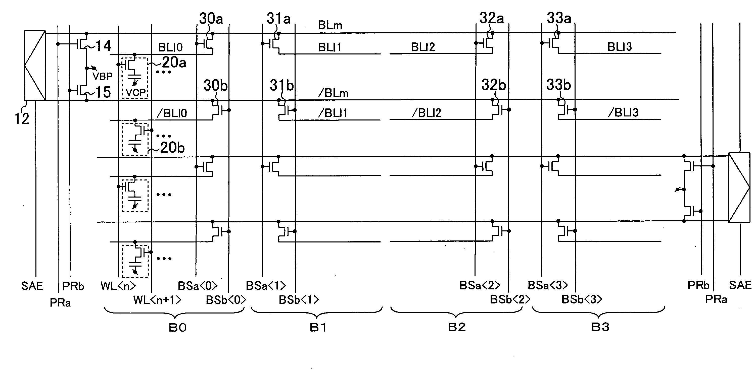
[0117]FIG. 3 is a circuit diagram for showing the configuration of a semiconductor memory device according to Modification 1. In the semiconductor memory device of FIG. 3, precharge transistors 40a, 40b, 41a, 41b, 42a, 42b, 43a, 43b, etc. working as local bit line precharge circuits are further provided in the semiconductor memory device of FIG. 1.

[0118]The precharge transistor 40a is connected between the precharge power source and the local bit line BLl0, and the precharge transistor 40b is connected between the precharge power source and the local bit line / BLl0.

[0119]The precharge transistor 40a supplies the bit line precharge voltage VBP to the local bit line BLl0 in accordance with a signal on a precharge control signal line PRa0>, and the precharge transistor 40b supplies the bit line precharge voltage VBP to the local bit line / BLl0 in accordance with a signal on a precharge control signal line PRb0>.

[0120]Similarly, the precharge transistor 41a is connected between the prec...

modification 2

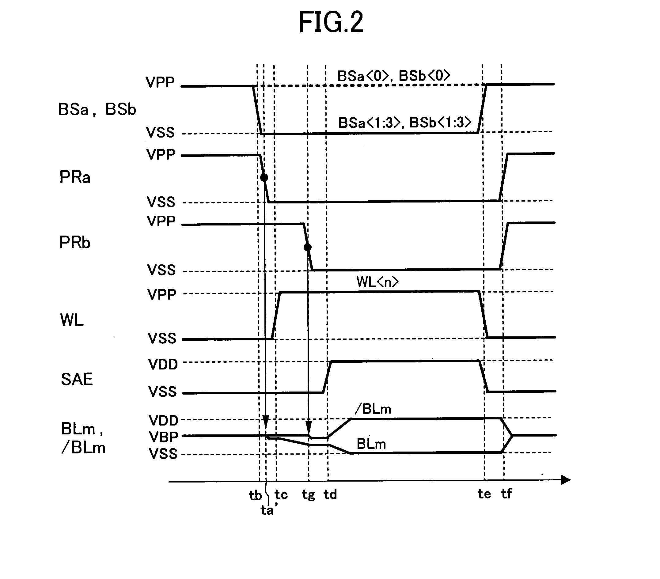
[0125]FIG. 5 is a timing chart for showing a read operation of a semiconductor memory device according to Modification 2.

[0126]In the read operation of FIG. 5, in the semiconductor memory device of FIG. 3, a signal the same as that on the precharge control signal line PRa is supplied to the precharge control signal line PRa0> for controlling the precharge transistor 40a for precharging the local bit line BLl0 connected to the memory cell to be accessed, and a signal the same as that on the precharge control signal line PRb is supplied to the precharge control signal line PRb0> for controlling the precharge transistor 40b for precharging the local bit line / BLl0 paired with the local bit line BLl0.

[0127]On the other hand, the precharge control signal lines PRa1:3> and PRb1:3>for controlling the precharge transistors 41a through 43a and 41b through 43b for precharging the local bit lines BLl1 through BLl3 and / BLl1 through / BLl3 other than the local bit lines related to the memory acc...

modification 3

[0129]FIG. 6 is a circuit diagram for showing the configuration of a semiconductor memory device according to Modification 3. The semiconductor memory device of FIG. 6 is obtained by further adding equalizing transistors 50, 51, 52, 53, etc. working as an equalizing circuit to the semiconductor memory device of FIG. 1.

[0130]The equalizing transistor 50 connects the local bit lines BLl0 and / BLl0 to each other in accordance with a signal on an equalizing control signal line EQ0>. Similarly, the equalizing transistor 51 connects the local bit lines BLl1 and / BLl1 to each other in accordance with a signal on an equalizing control signal line EQ1>, the equalizing transistor 52 connects the local bit lines BLl2 and / BLl2 to each other in accordance with a signal on an equalizing control signal line EQ2>, and the equalizing transistor 53 connects the local bit lines BLl3 and / BLl3 to each other in accordance with a signal on an equalizing control signal line EQ3>.

[0131]FIG. 7 is a timing ...


PUM


Abstract

A semiconductor memory device includes first and second global bit lines; first, second, third and fourth local bit lines; first, second, third and fourth hierarchical switches for respectively connecting the first global bit line and the first local bit line to each other, the second global bit line and the second local bit line to each other, the first global bit line and the third local bit line to each other, and the second global bit line and the fourth local bit line to each other; and first and second precharge circuits for respectively precharging the first and second global bit lines. When a memory cell connected to the first local bit line is read, the third hierarchical switch is turned off, and the first precharge circuit terminates its precharge operation after the third hierarchical switch is turned off and before a selected word line connected to the memory cell to be read is activated.

Description

CROSS-REFERENCE TO RELATED APPLICATIONS[0001]This application claims priority under 35 U.S.C. §119 on Patent Application No. 2006-111197 filed in Japan on Apr. 13, 2006, the entire contents of which are hereby incorporated by reference.BACKGROUND OF THE INVENTION[0002]The present invention relates to a semiconductor memory device, and more particularly, it relates to noise reduction and operation speed increase for a DRAM (dynamic random access memory) having a hierarchical bit line architecture.[0003]Recently, an embedded-DRAM is required to have a high degree of integration for realizing an SOC (system-on-a-chip) at low cost. It is a memory cell array including memory cells and a column of sense amplifiers that occupies most of the memory area. In order to realize the high degree of integration, the area of the memory cells has been reduced by refinement technique for a memory capacitor using a memory cell transistor and a high dielectric constant insulating film.[0004]On the othe...

Claims


Application Information

Patent Timeline
Patent Type & Authority Applications(United States)
IPC IPC(8): G11C7/00G11C7/02
CPCG11C7/02G11C7/12G11C2207/002G11C11/4094G11C11/4097G11C7/18
Inventor ILDA, MASAHISA
Owner PANASONIC SEMICON SOLUTIONS CO LTD
Why Eureka
Try Eureka