Photo-patterned carbon electronics

Active Publication Date: 2007-10-18
GULA CONSULTING LLC
View PDF15 Cites 28 Cited by
  • Summary
  • Abstract
  • Description
  • Claims
  • Application Information

AI Technical Summary

Problems solved by technology

In use, known semiconductors generate heat, and lose effectiveness when in high heat environments.
While the properties of these ca

Method used


Image

  • Photo-patterned carbon electronics
  • Photo-patterned carbon electronics
  • Photo-patterned carbon electronics

Examples


Embodiment Construction

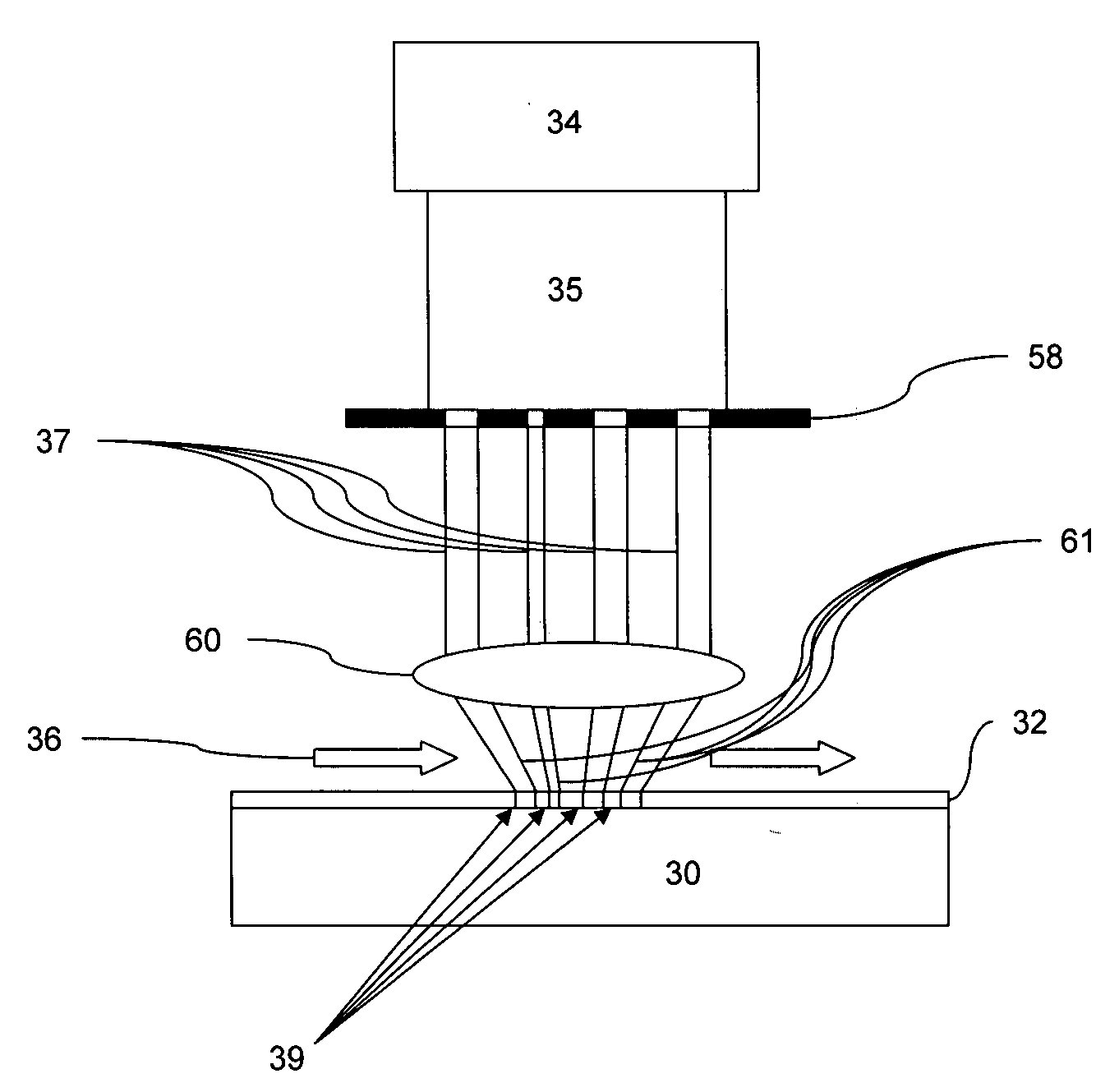
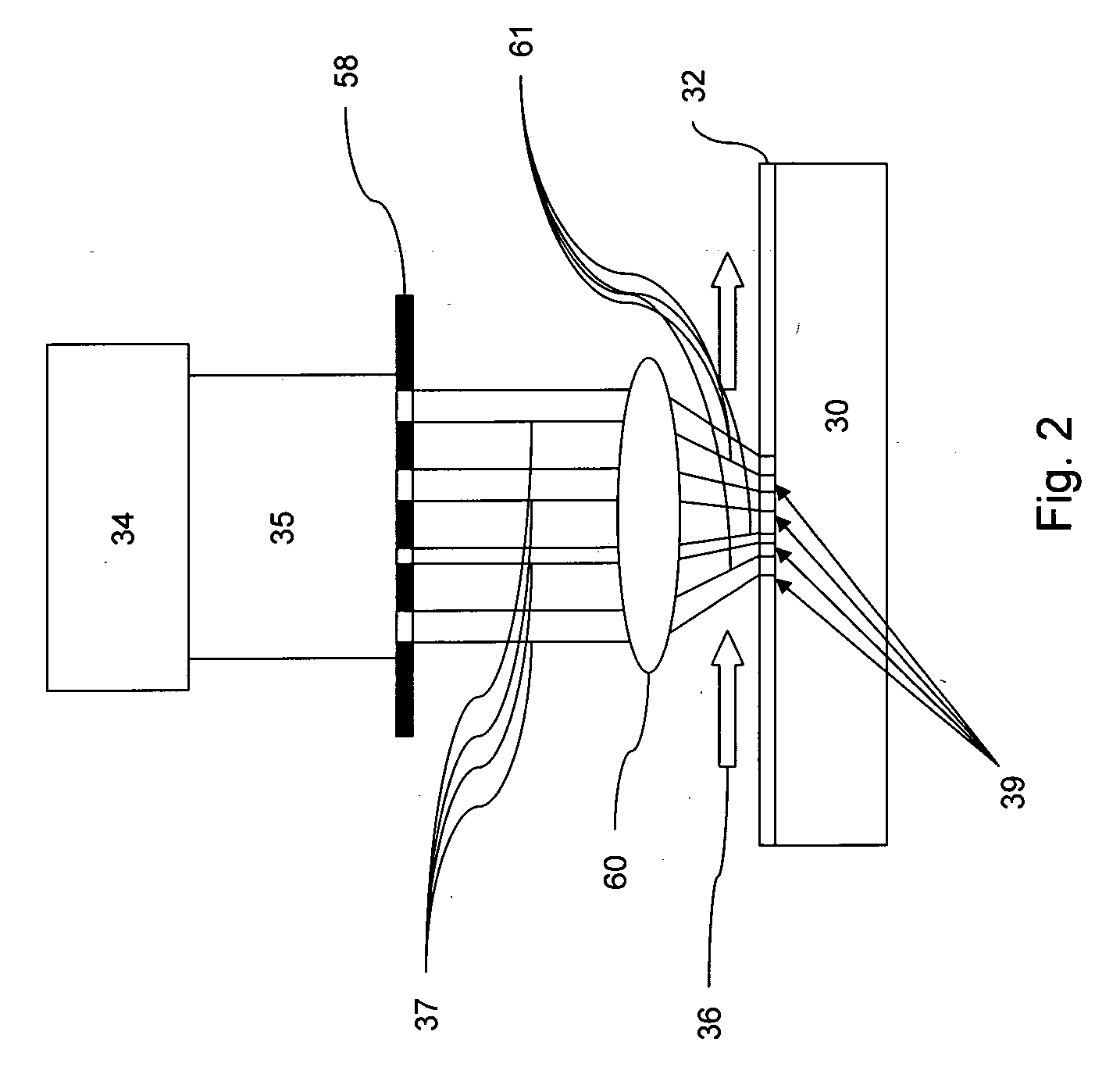
[0037] One embodiment of the present invention provides a method for the production of semiconductor component using deep ultraviolet (DUV) and extreme ultraviolet (EUV) radiation to induce the adsorption of doping agents into a carbon semiconductor.

[0038] In one such embodiment, photolithographic masking may be employed to expose patterns on a region of a workpiece to radiation in the UV radiation.

[0039] Diamond Like Carbon (DLC) thin films and Single wall nanotubes (SWNTs) have electrical and chemical properties making them especially suitable for semi conductor structures. In their un-doped state, DLCs are insulators, while SWNTs have a slight N-type bias. Diamond-like Carbon films have a high hardness, are chemically inert, and exhibit a high degree of thermal conductivity.

[0040] In one embodiment SWNTs may be doped by the introduction of halide or alkali metals as electron acceptors or donators, respectively. As uptake of dopant by both DLC thin films and SWNTs can be contro...


PUM

PropertyMeasurementUnit
Structureaaaaaaaaaa
Electrical resistanceaaaaaaaaaa
Semiconductor propertiesaaaaaaaaaa

Abstract

A system is provided for the manufacture of carbon based electrical components including, an ultraviolet light source; a substrate receiving unit whereby a substrate bearing a first layer of carbon based semiconductor is received and disposed beneath the ultraviolet light source; a mask disposed between the ultraviolet light source and the carbon based semiconductor layer; a doping agent precursor source; and environmental chemical controls, configured such that light from the ultraviolet light source irradiates a doping agent precursor and the first carbon layer.

Description

FIELD OF THE INVENTION [0001] The invention relates to the manufacture of carbon based semiconductor components, and more particularly, to photo patterned carbon electrical components and a method for the manufacture thereof. BACKGROUND OF THE INVENTION [0002] Known methods of forming semiconductor electronic components require successive masking and photo-etching steps through which horizontal structures and doped layers of semi-conductors are built up from a substrate. The components thus produced are typically comprised of silicon, gallium, indium, and other p-bock semi-metallic elements to which dopants are introduced to effect changes in the electronic configuration of the semiconductor crystal. In use, known semiconductors generate heat, and lose effectiveness when in high heat environments. Consequently, cooling systems, such as heat sinks and fans are typically be employed to prevent heat damage to the electronic component, and in high speed and high voltage applications, sp...

Claims


Application Information

Patent Timeline
IPC IPC(8): C25B11/00C25D17/10C25C7/02B05D5/12
CPCB82Y10/00C23C10/02C23C16/042C23C16/26H01L51/0048C23C26/00H01L51/0015H01L51/002C23C16/483H10K71/211H10K71/30H10K85/221
Inventor CAROTHERS, DANIEL N.THOMPSON, RICK
Owner GULA CONSULTING LLC
Why Eureka
Try Eureka