P-N Junction-Type Compound Semiconductor Light-Emitting Diode

Inactive Publication Date: 2007-10-25
SHOWA DENKO KK
View PDF12 Cites 7 Cited by
  • Summary
  • Abstract
  • Description
  • Claims
  • Application Information

AI Technical Summary

Benefits of technology

[0015] According to the first aspect of this invention, a boron phosphide-based Group III-V compound semiconductor layer possessing a band gap exceeding that of a Group III nitride semiconductor forming an n-type active layer at room temperature is formed on a Group III nitride semiconductor layer containing a p-type impurity. Therefore, the first aspect of the invention is capable of suppressing the absorption of emission from a light-emitting layer by an electroconductive layer, acquiring an enhanced transparency to the emission, improving efficiency of the passage of the emission to the exterior and exalting the luminance of the diode.
[0016] Further, in the first aspect, the boron phosphide-based Group III-V compound semiconductor layer on the p-type impurity-containing Group III nitride semiconductor layer is formed of a layer showing a p-type electroconductivity in an undoped state. Therefore, the first aspect of the invention is capable of securing a high carrier concentration in the undoped state and lowering the electric resistance of the layer. As a result, it can form an ohmic electrode of a low contact resistance and realize a p-n junction-type compound semiconductor diode endowed with a low forward voltage and an excellent rectifying property at a reverse voltage.
[0019] According to the fourth aspect of this invention, an ohmic positive electrode is disposed on a boron phosphide-based semiconductor layer formed of monomeric boron phosphide (BP) having a band gap of 2.8 eV or more and 5.0 eV or less at room temperature and a component element number of 3 (3 elements) or less. Therefore, the fourth aspect of the invention is capable of contributing to the provision of a p-n junction-type compound semiconductor light-emitting diode making convenient the extraction of emission to the exterior and abounding in the intensity of emission.
[0020] According to the fifth aspect of the invention, a boron phosphide-based semiconductor layer is configured with monomeric boron phosphide (BP) having a carbon atomic concentration of 6×1018 cm3 or less. Therefore, the fifth aspect of the invention is capable of providing a contact layer that affords optical transparency proper for the extraction of emission to the exterior and an excellent ohmic contact property and, as a result, providing a p-n junction-type compound semiconductor light-emitting diode withy low forward voltage and high intensity of emission.

Problems solved by technology

The aluminum gallium nitride (AlXGaYN: 0≦X, Y≦1, X+Y=1), a wide band gap material heretofore used for formation of a clad layer, however, brings a problem of encountering difficulty in forming an electroconductive layer [a layer for passing a device operation current (the current to operate a light-emitting device) from the positive electrode to the light-emitting layer] showing sufficiently low resistance.
Even GaN which is utilized for forming a contact layer has not fully matured into a material suitable for a p-type electroconductive layer of low resistance.
Thus, the acquisition of a light-emitting device of high emission has been obstructed by the fact that the device operation current allows no fully satisfactory planar diffusion in the light-emitting layer.
An effort to adopt the conventional BP layer of a narrow band gap as a contact layer and dispose it so as to direct the emission toward the exterior results in merely the absorption of emission and inconveniencing the acquisition of a light-emitting device of high luminance.

Method used


Image

  • P-N Junction-Type Compound Semiconductor Light-Emitting Diode
  • P-N Junction-Type Compound Semiconductor Light-Emitting Diode
  • P-N Junction-Type Compound Semiconductor Light-Emitting Diode

Examples


example

[0039] This invention will be specifically described below by citing as an example the case of fabricating a p-n junction-type compound semiconductor LED utilizing a monomeric boron phosphide semiconductor layer formed on a p-type gallium nitride (GaN) layer.

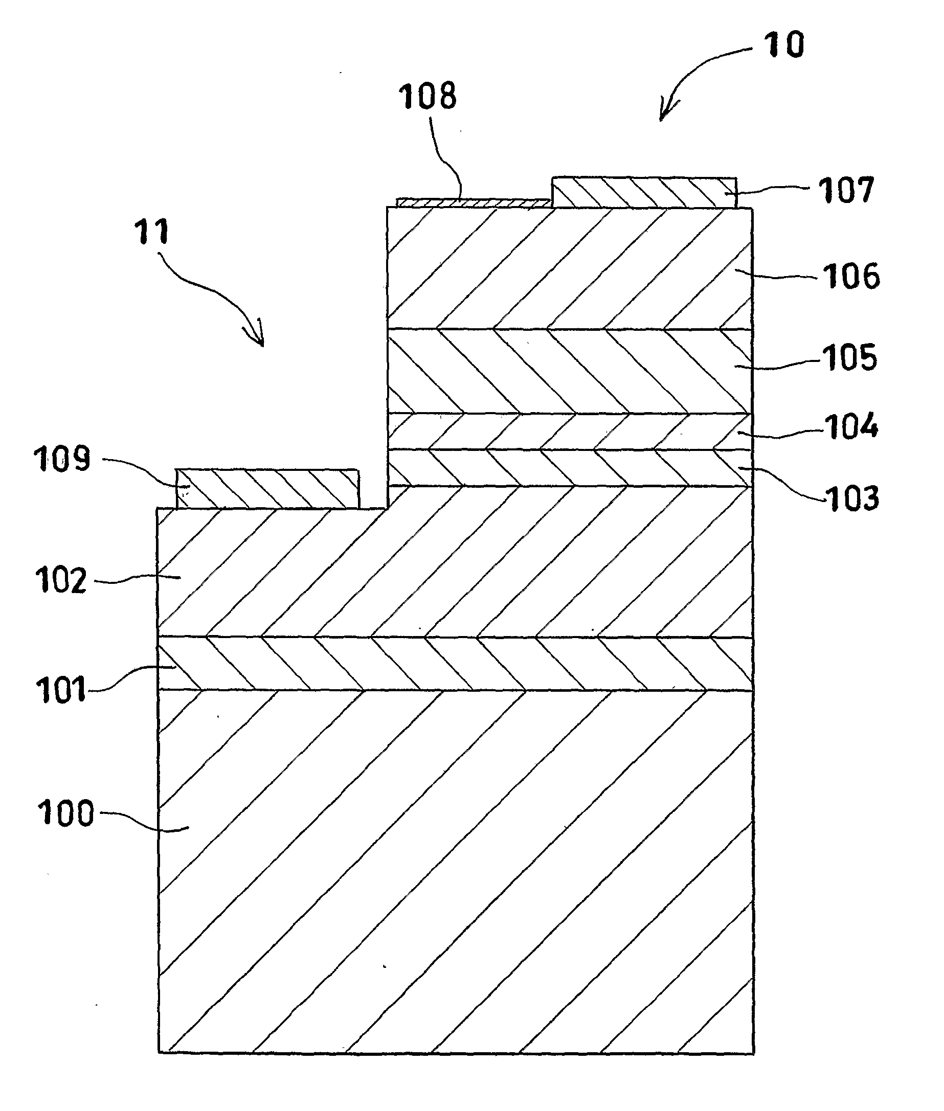
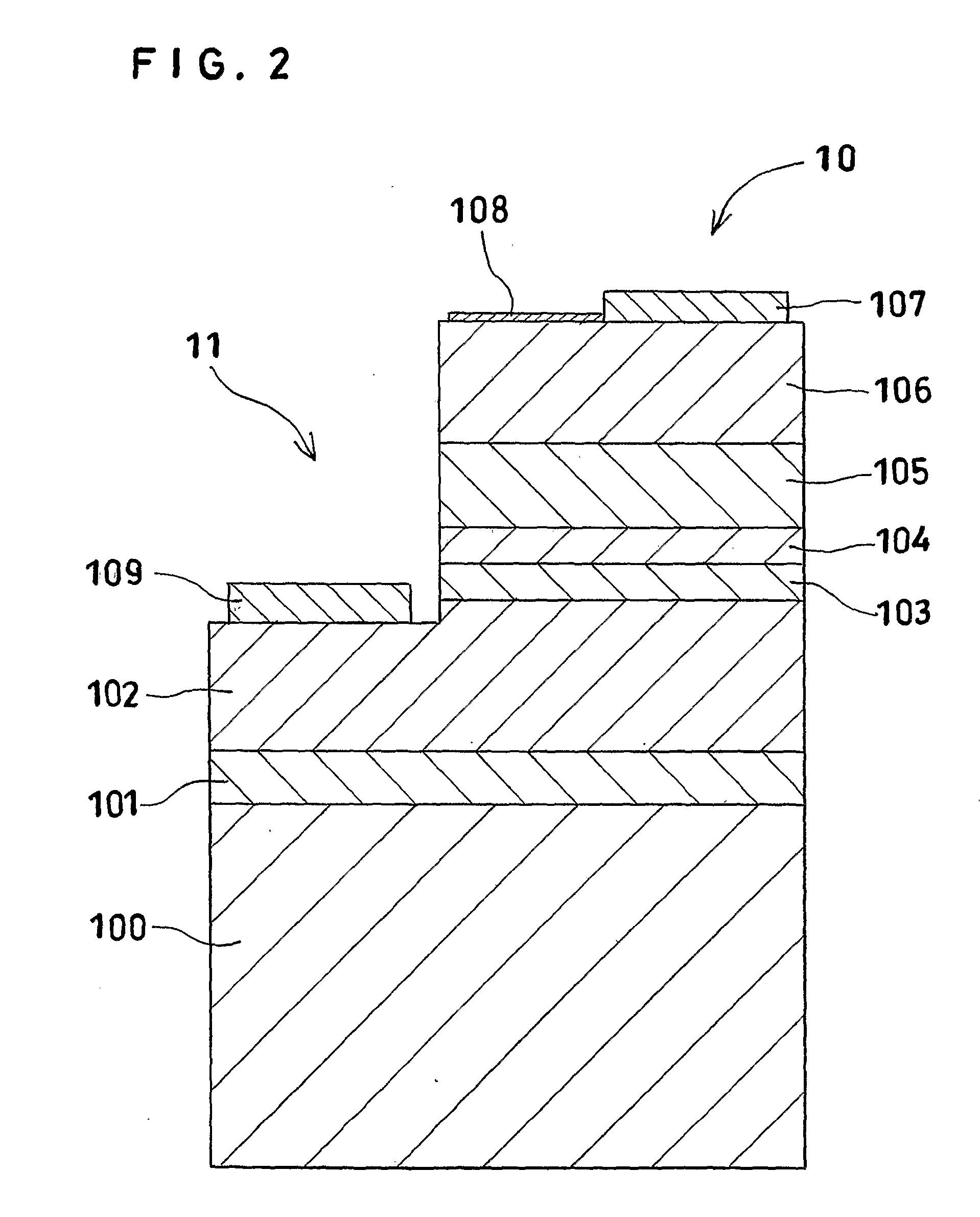
[0040]FIG. 2 schematically shows the cross-sectional view of a stacked structure 11 used for the fabrication of an LED 10 of a double hetero (DH) junction structure. FIG. 3 illustrates a schematic plan view of the LED 10.

[0041] The stacked structure 11 was formed by stacking on a (0001)-sapphire (α-Al2O3 single crystal) substrate 100, an undoped buffer layer 101 formed of GaN, a lower clad layer 102 formed of silicon (Si)-doped n-type GaN (n=7×1018 cm−3, layer thickness (t)=3 μm), a light-emitting layer 103 containing an undoped n-type Ga0.86In0.14N layer, an upper clad layer (Group III nitride semiconductor layer) 104 formed of Mg-doped p-type Al0.06Ga0.94N (p=3×1017 cm−3, t=0.08 μm), and a p-type layer (Group III nitride sem...


PUM


Abstract

In a p-n junction-type compound semiconductor light-emitting diode provided on a crystal substrate with at least an n-type active layer formed of a Group m nitride semiconductor as a light emitting layer, and with a Group m nitride semiconductor layer containing a p-type impurity on the n-type active layer, the diode has a boron phosphide-based Group III-V compound semiconductor layer possessing a band gap exceeding that of the Group m nitride semiconductor forming the n-type active layer at room temperature and exhibiting a p-type electroconductivity in an undoped state deposited on the p-type impurity-containing Group III nitride semiconductor layer, and has an ohmic positive electrode joined to a surface of the boron phosphide-based Group III-V compound semiconductor layer.

Description

CROSS REFERENCE TO RELATED APPLICATIONS [0001] This application is an application filed under 35 U.S.C. § 111 (a) claiming the benefit pursuant to 35 U.S.C. § 119 (e) (1) of the filing dates of Provisional Application No. 60 / 572,268 filed May 19, 2004 and Japanese Patent Application No. 2004-137229 filed May 6, 2004 pursuant to 35 U.S.C. § 111 (b). TECHNICAL FIELD [0002] This invention relates to a p-n junction-type compound semiconductor light-emitting diode provided on a crystal substrate with at least an n-type active (light-emitting) layer formed of a Group III nitride semiconductor and with a Group III nitride semiconductor layer containing a p-type impurity on the n-type active layer. BACKGROUND ART [0003] As light-emitting devices for mainly emitting blue through green light, the light-emitting diode (LED) and laser diode (LD) using as a Group III-V compound semiconductor (Group III nitride semiconductor) layer containing nitrogen (N), for example, as a Group V component elem...

Claims


Application Information

Patent Timeline
IPC IPC(8): H01L33/00H01L33/26H01L33/32H01S5/042H01S5/30H01S5/323
CPCH01L33/26H01L33/32H01S5/32341H01S5/3054H01S5/0421
Inventor ODAWARA, MICHIYAUDAGAWA, TAKASHI
Owner SHOWA DENKO KK
Why Eureka
Try Eureka