Method and apparatus for irradiating laser
a laser and laser technology, applied in the direction of optical radiation measurement, semiconductor/solid-state device testing/measurement, instruments, etc., can solve the problems of reducing the grain size of the resultant polycrystalline-si film, preventing the improvement of the throughput of forming the polycrystalline-si film, and not achieving suitable grain size, etc., to achieve the effect of improving the throughput and g siz
- Summary
- Abstract
- Description
- Claims
- Application Information
AI Technical Summary
Benefits of technology
Problems solved by technology
Method used
Image
Examples
first embodiment
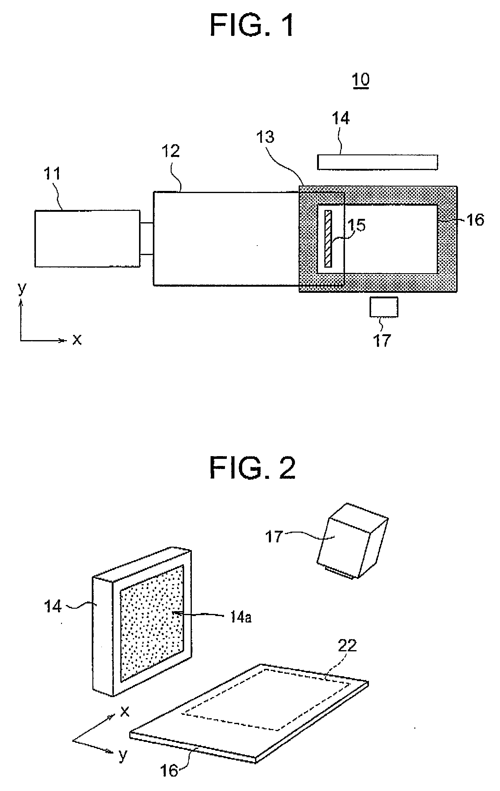
[0027]FIG. 1 is a top plan view showing the configuration of a laser irradiation apparatus, generally designated by numeral 10, for use in a laser irradiation method according to the present invention. The laser irradiation apparatus 10 includes a laser source 11, an optical system 12, a stage 13, a surface-light source unit 14 and an optical sensor configured by a charge coupled device 17. The laser irradiation apparatus 10 is used for melting and recrystallizing an amorphous-Si film formed on a surface of a substrate 16 to form a polycrystalline-Si film therefrom.
[0028]The laser source 11, which is an excimer laser device, generates a pulse laser having a predetermined lasing frequency toward the direction denoted by “x”. The optical system 12 forms the laser 15 irradiated from the, laser source 11 into an elongated rectangular shape, or linear shape, extending along the direction denoted by “y”. The substrate 16 is placed on the stage 13, and the rectangular-shaped laser is irrad...
second embodiment
[0039]FIG. 7 is a flowchart showing the procedure of a method for judging the size uniformity in a laser irradiation process according to the present invention, In the method of the present embodiment, judged is the uniformity of the grain size of the polycrystalline-Si film formed by a laser irradiation. First, the laser irradiation apparatus shown in FIG. 1 is used, where the substrate for a product is placed on the stage 13, and the actual irradiation is performed to form a polycrystalline-Si film of the TFT devices (step S21). To form the polycrystalline-Si film, the irradiation intensity of laser is set lower than the microcrystallization intensity.
[0040]Next, while allowing the surface-light source unit 14 to illuminate the target irradiation area which has been irradiated by laser, the charge coupled device 17 picks-up the image of the target irradiation area in block (step S22). A plurality of judgment regions are set within the target irradiation area, and the chromaticity ...
PUM
 Abstract
Description
Claims
Application Information
 - R&D Engineer
- R&D Manager
- IP Professional
- Industry Leading Data Capabilities
- Powerful AI technology
- Patent DNA Extraction
Browse by: Latest US Patents, China's latest patents, Technical Efficacy Thesaurus, Application Domain, Technology Topic, Popular Technical Reports.
© 2024 PatSnap. All rights reserved.Legal|Privacy policy|Modern Slavery Act Transparency Statement|Sitemap|About US| Contact US: help@patsnap.com


