Semiconductor device and semiconductor device layout designing method

a semiconductor device and semiconductor technology, applied in the direction of resonant antennas, instruments, burglar alarm mechanical actuation, etc., can solve the problems of more serious antenna damage, plasma charging damage, and damage to the semiconductor elements, so as to achieve the planarization within the chip and avoid antenna damage , secure the effect of wiring efficiency

Active Publication Date: 2007-11-01
PANASONIC SEMICON SOLUTIONS CO LTD
View PDF12 Cites 2 Cited by
  • Summary
  • Abstract
  • Description
  • Claims
  • Application Information

AI Technical Summary

Benefits of technology

[0019]In the above invention, each wiring is provided in the wiring layer in which the first wiring connected to the gate is formed so as not to cover the active region of the antenna protection element. Accordingly, the amount of the light to the antenna protection element can be secured until the wiring layer is formed, thereby allowing the antenna protection element to exert sufficient performance for protecting the semiconductor device from antenna damage. On the other hand, the second wiring provided in the upper layer of this wiring layer is provided so as to cover at least a part of the active region of the antenna protection element. Because any wiring layers formed above the wiring layer in which the first wiring is formed causes no antenna damage at the gate, it is allowed to be overlaid with the antenna protection element. This avoids antenna damage and secures wiring resources.
[0070]As described above, according to the present invention, a semiconductor device which avoids antenna damage, secures wiring efficiency, and achieves planarization within a chip can be attained with ease.

Problems solved by technology

While, there arises a serious problem of flaws of semiconductor elements called plasma charging damage, which is caused due to the plasma process.
Further, scale down of the thicknesses of the gate oxide films accompanied by miniaturization in the process technology makes the antenna damage more serious.
Unless the area ratio is satisfied, the etching rate varies and the surface of the substrate is planarized insufficiently in the CMP process, thereby achieving insufficient process accuracy.
In both Patent Document 1 and Patent Document 2, however, any dummy pattern cannot be arranged above the antenna protection element, thereby making the area ratio around the antenna protection element small to achieve insufficient process accuracy.
Further, since miniaturization in process technology, such as scale down in thicknesses of gate oxide films accompanies more serious antenna damage, the number and the area of the antenna elements to be arranged is liable to increase.

Method used


Image

  • Semiconductor device and semiconductor device layout designing method
  • Semiconductor device and semiconductor device layout designing method
  • Semiconductor device and semiconductor device layout designing method

Examples


embodiment 1

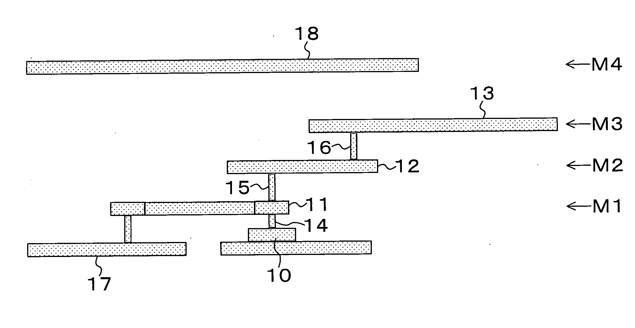
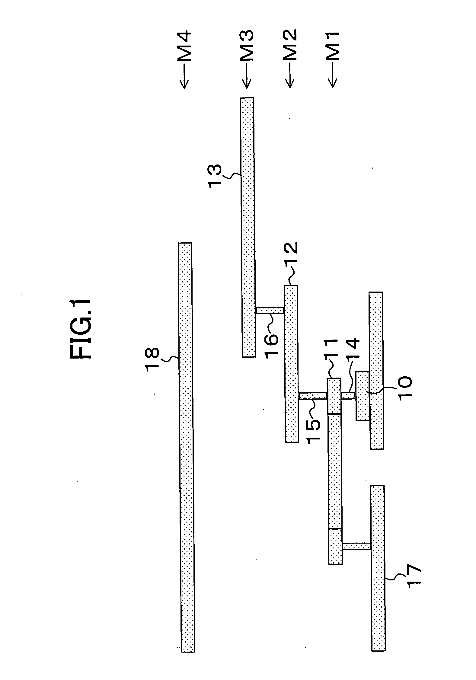
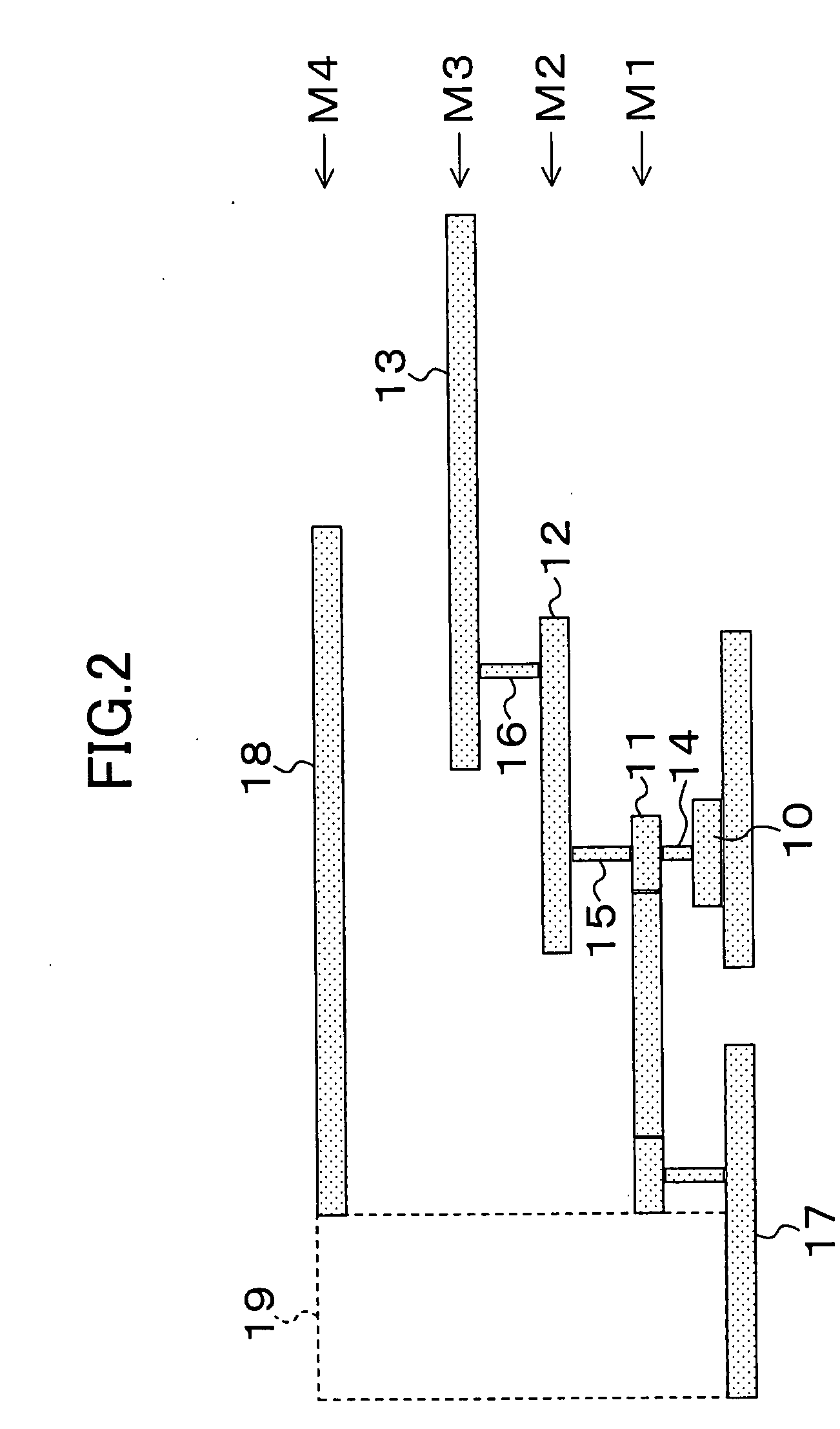
[0127]FIG. 1 is a sectional view showing a configuration of a semiconductor device according to Embodiment 1 of the present invention. In FIG. 1, reference numeral 10 denotes a gate, 11 denotes a wiring in a metal wiring layer M1, 12 denotes a wiring in a metal wiring layer M2, 13 denotes a wiring in a metal wiring layer M3, 14 denotes a contact which connects the gate 10 and the wiring 11, 15 denotes a first via which connects the wiring 11 and the wiring 12, 16 denotes a second via which connects the wiring 12 and the wiring 13, and 17 denotes an antenna protection element (a diffusion region). The antenna protection element 17 is connected electrically to the gate 10 by means of the wiring 11 in the metal wiring layer M1.

[0128]The wirings 11, 12, 13 form a first wiring connected to the gate 10. In a metal wiring layer M4 above the first wiring, a wiring 18 as a second wiring is formed.

[0129]FIG. 2 is a sectional view showing a configuration of a conventional semiconductor device,...

embodiment 2

[0158]FIG. 13 shows a general layout of a semiconductor device. In FIG. 13, a plurality of cells including antenna protection elements 131 are arranged, and source wirings 132, 134, 135 and signal wirings 133, 136, 137 are routed in layers above the cells. In general, as shown in FIG. 13, source wirings and signal wirings are formed in layers above antenna protection elements in many cases. For example, the source wiring 134 is formed in the layer above the antenna protection element 131. This reduces the amount of the UV light irradiated to the active region, lowering the performance of the antenna protection element.

[0159]In Embodiment 1, an area where wirings and dummy patterns can be arranged is estimated through antenna damage verification on the assumption of the performance of the antenna protection element from an overlap area between the antenna protection element and a wiring thereabove after completion of routing.

[0160]In some layouts, however, error would be caused in an...

embodiment 3

[0166]In Embodiment 2, the amount of the UV light irradiated to the antenna protection element is increased by changing the shape of a wiring pattern above an antenna protection element, for example, by deleting a part of the wiring which is located above the antenna protection element. As to a signal wiring above the antenna protection element, however, change in shape and cutting are difficult in view of the timing and the logic. Further, when an antenna protection element is arranged in a region congested with signal wirings, the area of the antenna protection element to which the UV light is irradiated reduces to lower the performance of the antenna protection element.

[0167]In the present embodiment, the UV light irradiated to the antenna protection element is secured by limiting in advance an amount of wirings running above an antenna protection element.

[0168]FIG. 17 shows a layout of a semiconductor device. FIG. 17 indicates a virtually set window 171 in the same layout as tha...


PUM


Abstract

In each wiring layer in which wirings connected to a gate is formed, wirings are routed so as not to cover the active region of an antenna protection element. A wiring formed in an upper wiring layer is routed so as to cover at least a part of the active region of the antenna protection element.

Description

CROSS REFERENCE TO RELATED APPLICATIONS[0001]This Non-provisional application claims priority under 35 U.S.C. § 119(a) on Patent Application No. 2006-126083 filed in Japan on Apr. 28, 2006, the entire contents of which are hereby incorporated by reference.BACKGROUND OF THE INVENTION[0002]1. Field of the Invention[0003]The present invention relates to a semiconductor device including an antenna protection element for avoiding antenna damage and a layout designing method thereof.[0004]2. Background Art[0005]In association with recent miniaturization in semiconductor manufacturing technology, employment of a plasma process typified by plasma etching and plasma CVD becomes general in device manufacturing processes. While, there arises a serious problem of flaws of semiconductor elements called plasma charging damage, which is caused due to the plasma process.[0006]The plasma charging damage is called also antenna damage and serves as a factor of an increase in gate leakage current, degr...

Claims


Application Information

Patent Timeline
Patent Type & Authority Applications(United States)
IPC IPC(8): H01L23/02G08B13/14H01Q9/04
CPCH01L27/118H01L27/0203
Inventor SHIMADA, JUNICHIKIMURA, FUMIHIROMATSUMURA, YOICHIOHASHI, TAKAKOIWAUCHI, NOBUYUKIFUJINO, TAKEYAARAKI, TAKAYUKIHASHIMOTO, YUKIJIYASUI, TAKUYATAGUCHI, HIROFUMI
Owner PANASONIC SEMICON SOLUTIONS CO LTD
Why Eureka
Try Eureka