

Optical sensor and method for optically inspecting surfaces
a technology of optical inspection and optical sensor, which is applied in the direction of optical radiation measurement, instruments, photometry, etc., can solve the problems of inability to use a one hundred percent examination method of flat glass, and the defects which can be identified with this technology lie in the range of a few micrometers, so as to achieve uniform detection sensitivity
- Summary
- Abstract
- Description
- Claims
- Application Information
AI Technical Summary
Benefits of technology
Problems solved by technology
Method used
Image

Examples
Embodiment Construction
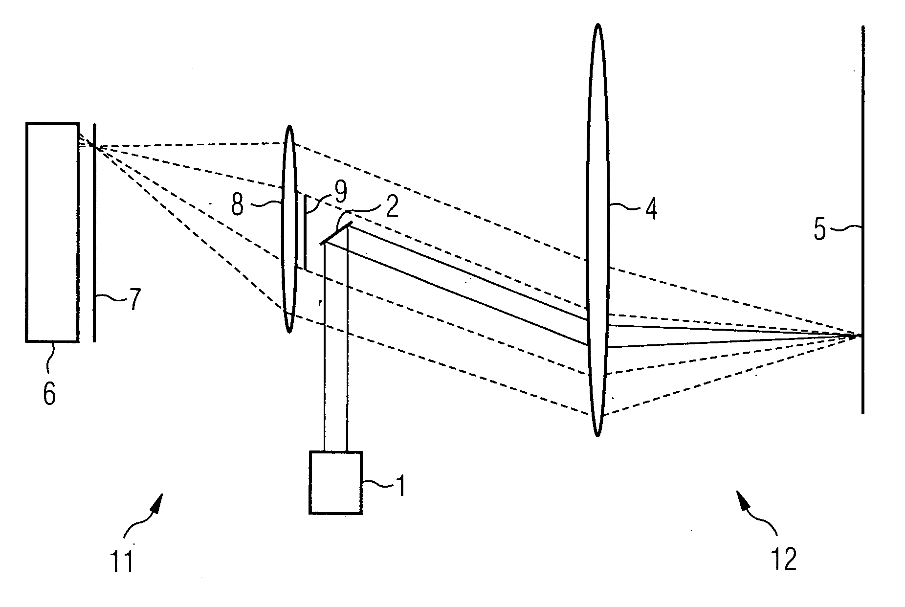
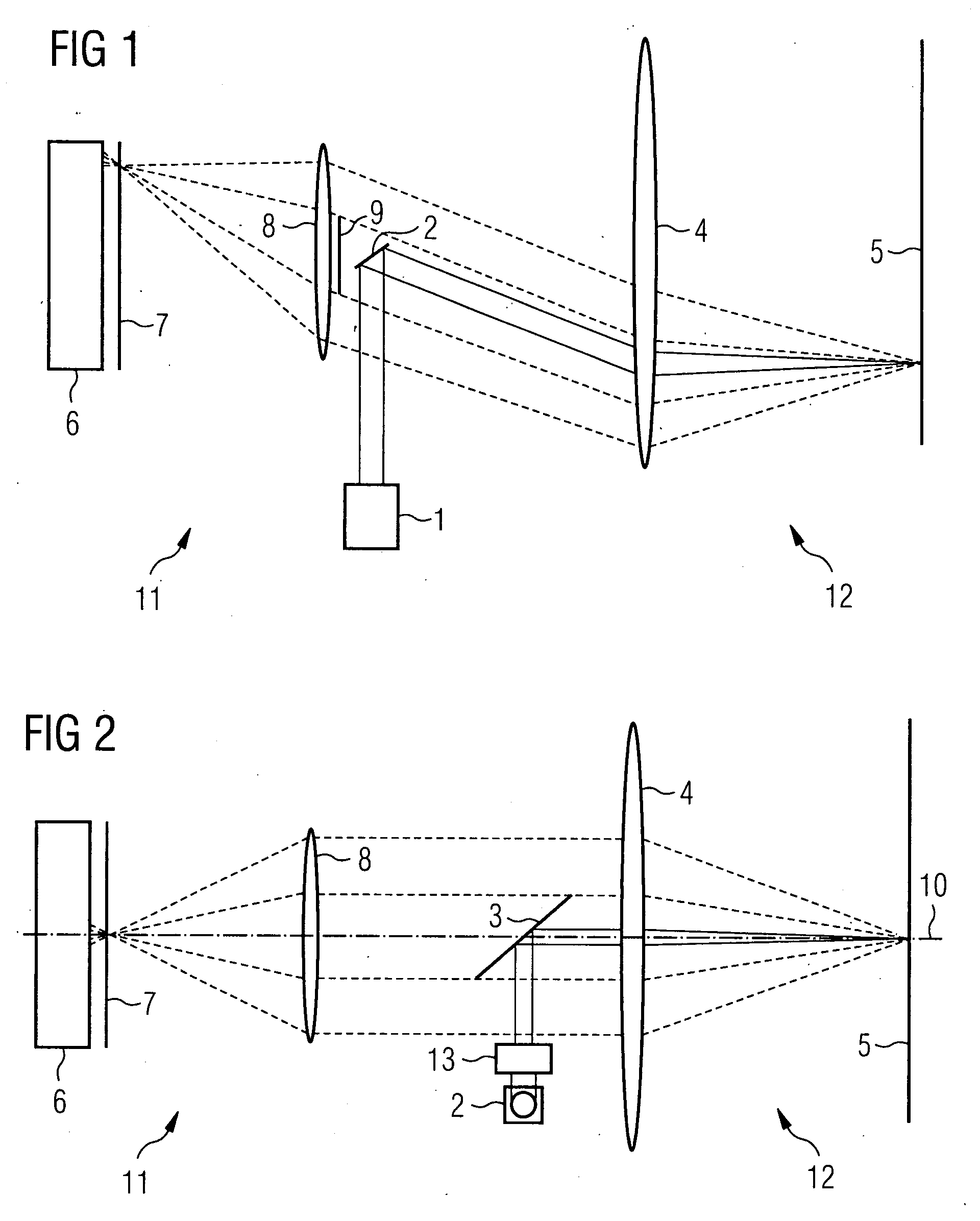
[0015]FIG. 1, which reproduces the main design of a described sensor, shows that the collimated light of a laser is deflected from a scanner in a specific angular range. A laser 1 generates a laser beam, which is deflected by means of a scanning mirror 2. A telecentric optical scanning system 4 focuses the deflected light onto the smooth surface 5 to be examined or onto a glass specimen. The light beams hit the surface perpendicularly, and as a result of the deflection of the scanning mirror, the laser focus on the surface describes a line. The laminar scanning of the glass specimen is achieved by the infeed of the specimen perpendicular to the scanning line. The scattered light reflected by the glass surface is collimated by the telecentric optical scanning system 4 and is focused onto a slit diaphragm 7 using a downstream optical detector system 8. The focused light flows through the slit diaphragm 7 and hits the receiving surface of a photomultiplier 6. The slit diaphragm 7 arran...
PUM
| Property | Measurement | Unit |
|---|---|---|
| angle | aaaaa | aaaaa |
| depth of field | aaaaa | aaaaa |
| thickness | aaaaa | aaaaa |
Abstract
Description
Claims
Application Information