Multi-functional chalcogenide electronic devices having gain

a technology of electronic devices and chalcogenide, applied in the direction of bulk negative resistance effect devices, semiconductor devices, electrical appliances, etc., can solve the problems of silicon entering the quantum regime of behavior, silicon further reducing the feature size, and no longer functioning according to the fundamental behavior of silicon, etc., to achieve the effect of greater functionality

Active Publication Date: 2007-11-22
OVONYX MEMORY TECH LLC
View PDF16 Cites 9 Cited by
  • Summary
  • Abstract
  • Description
  • Claims
  • Application Information

AI Technical Summary

Benefits of technology

[0007]The instant invention provides electronic devices that can be used in the construction of novel computers and computing devices having greater functionality than today's conventional computers. The instant devices are not based on silicon, but rather on chalcogenide phase change materials that can be reversibly transformed ...

Problems solved by technology

Further decreases in feature size, however, are deemed problematic because sizes below about 0.10 micron are expected lead to a change in the fundamental behavior of silicon.
More specifically, as the dimensions of silicon devices decrease to tens of nanometers and below, silicon enters the quantum regime of behavior and no longer functions according to the classical physics that governs macroscopic objects.
Consequences of tunneling include leakage of current as electrons escape from one device to neighboring devices and a loss of independence of devices as the state of one device influences the state of neighboring devices.
In addition to fundamental changes in the behavior of silicon, further decreases in the dimensions of silicon devic...

Method used


Image

  • Multi-functional chalcogenide electronic devices having gain
  • Multi-functional chalcogenide electronic devices having gain
  • Multi-functional chalcogenide electronic devices having gain

Examples


example 1

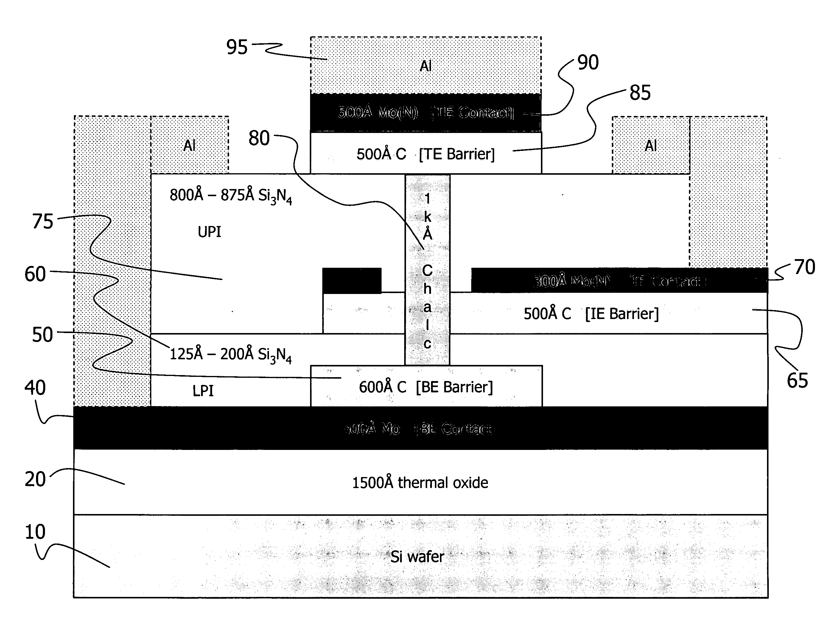
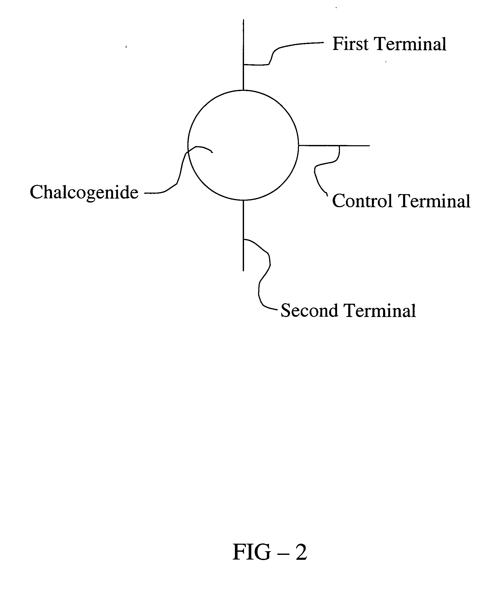
[0063]An example of a device structure according to the instant invention is shown in FIG. 3. FIG. 3 shows a cross-sectional view of a three terminal device structure. A plurality of these devices was formed on a silicon wafer. The devices and layers on the wafer were formed using conventional sputter deposition, etching, and lithography techniques. The structure includes a silicon wafer substrate 10, a silicon oxide layer 20, a bottom terminal that includes a conductive layer 40 formed from Mo and a carbon layer 50, a lower Si3N4 insulating region 60, a control terminal that includes a carbon layer 65 and a Mo layer 70, an upper Si3N4 insulating layer 75, a chalcogenide material 80 contained in the pore region of the device, a top terminal that includes a carbon layer 85 and a conductive layer 90 that includes Mo, and Al layers 95. In this example, the chalcogenide material 80 is an Se—Te chalcogenide alloy having an approximate composition Si5Ge11As28Te34Se21S. Typical layer thick...

example 2

[0065]In this example, a device having a symmetric design was fabricated according to the process described in EXAMPLE 1 hereinabove. In the symmetric design, the upper insulating layer 75 and lower insulating layer 60 both had a thickness of 500 Å, so that the control terminal 70 was positioned symmetrically between top terminal 90 and lower terminal 30. Other features of the symmetric device are as described in EXAMPLE 1. The separation between control terminal 70, top terminal 90 and lower terminal 30 is believed to be large enough to prevent a significant interaction between the space-charge regions emanating from the three terminals.

example 3

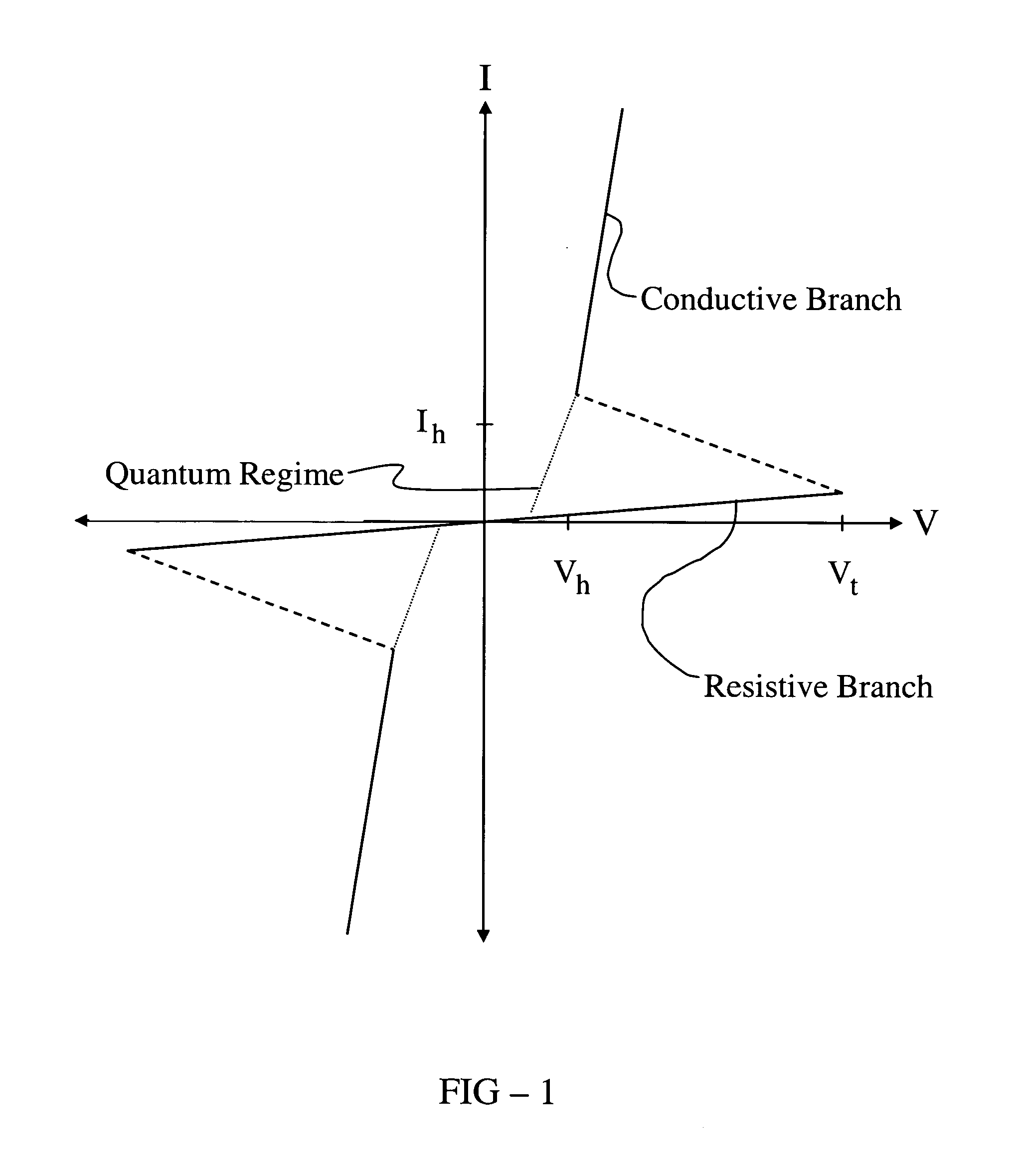
[0066]In this example, a demonstration of the latching and non-latching modes of operation of the device described in EXAMPLE 1 is provided. An illustration of operation in latching mode is presented in FIG. 4, which shows the time variation of the voltage between the top and bottom terminals of the device before and after application of a voltage signal between the control terminal and bottom terminal. FIG. 4 includes two data curves: one, depicted in diamond symbols, that shows the voltage between the top and bottom terminals as a function of time and another, depicted in square symbols, that shows the voltage between the control and bottom terminals as a function of time. At the outset of the experiment, a signal of approximately 2V was applied between the top and bottom terminals and no signal was applied between the control terminal and the bottom terminal. The signal applied between the top and bottom terminals was an insufficient voltage to cause a switching event to occur. W...


PUM


Abstract

Multi-functional electronic switching and current control device comprising a chalcogenide material. The devices include a load terminal, a reference terminal and a control terminal. Application of a control signal to the control terminal permits the device to function in one or more of the following modes reversibly: (1) a gain mode in which gain is induced in the current passing between the load and reference terminals; (2) a conductivity modulation mode in which the conductivity of the chalcogenide material between the load and reference terminals is modulated; (3) a current modulation mode in which the current or current density between the load and reference terminals is modulated; and/or (4) a threshold modulation mode in which the voltage required to switch the chalcogenide material between the load and reference terminals from a resistive state to a conductive state is modulated. The devices may be used as interconnection devices or signal providing devices in circuits and networks.

Description

FIELD OF THE INVENTION[0001]This invention relates generally to chalcogenide electronic devices. More particularly, this invention relates to modification, amplification and multi-functional switching devices. Most particularly, this invention pertains to multi-terminal switching and control devices in which the application of a control signal at a control terminal regulates the operation of the device to provide new functionality, in a non-silicon computing platform, that surpasses a transistor.BACKGROUND OF THE INVENTION[0002]Today's electronic devices rely on conventional silicon technology. With silicon technology, one can fabricate the electronic components (e.g. transistors, diodes, switches, memory, integrated circuits and processors) needed to produce modern computers and consumer electronic products. Silicon-based electronics have enjoyed great success in the market place and have provided a number of conveniences that have greatly simplified everyday life.[0003]The growth ...

Claims


Application Information

Patent Timeline
IPC IPC(8): H01L29/06H01L31/00
CPCH01L45/065H01L45/1206H01L45/1233H01L45/144H01L45/142H01L45/143H01L45/141
Inventor OVSHINSKY, STANFORD R.
Owner OVONYX MEMORY TECH LLC
Why Eureka
Try Eureka