Patterning A Single Integrated Circuit Layer Using Multiple Masks And Multiple Masking Layers

a technology of integrated circuits and masks, applied in the field of forming features of integrated circuits, can solve the problems of phase shifting alone generating only poorly defined wafer features, requiring yet more complex layout patterns at the mask stage, and leaving the photoresist coating unexposed in these regions, etc., to achieve the effect of facilitating the use of rets, improving yield and small feature siz

Active Publication Date: 2007-11-29
SYNOPSYS INC
View PDF3 Cites 137 Cited by
  • Summary
  • Abstract
  • Description
  • Claims
  • Application Information

AI Technical Summary

Benefits of technology

[0025]Note that the multiple masks and multiple masking layers result in fine-line patterns, wherein each fine-line pattern includes fine-line features that are oriented in a single direction and that are laid out on a regular grid. This positioning can advantageously minimize feature variations for improved yield as well as facilitate the use of RETs to achieve the most aggressively small feature sizes for optimized circuit performance. Moreover, multiple masks and multiple masking layers can significantly reduce mask complexity, thereby achieving high-fidelity layer patterning at lower overall cost.

Problems solved by technology

In contrast, light is blocked by the opaque regions of the binary mask, thereby leaving the photoresist coating unexposed in these regions.
Smaller technology nodes require yet more complex layout patterns at the mask stage.
However, at this technology node, phase shifting by itself can only generate a poorly defined wafer feature 216.
Notably, such complex RETs can make sub-wavelength resolution possible, but at increased design and manufacturing (e.g. photolithography) cost.
Unfortunately, because of the widening gap between the wavelength of light and the minimum feature size with technology advancement over time, this cost is expected to significantly increase with each new generation of integrated circuit technology.

Method used


Image

  • Patterning A Single Integrated Circuit Layer Using Multiple Masks And Multiple Masking Layers
  • Patterning A Single Integrated Circuit Layer Using Multiple Masks And Multiple Masking Layers
  • Patterning A Single Integrated Circuit Layer Using Multiple Masks And Multiple Masking Layers

Examples


Embodiment Construction

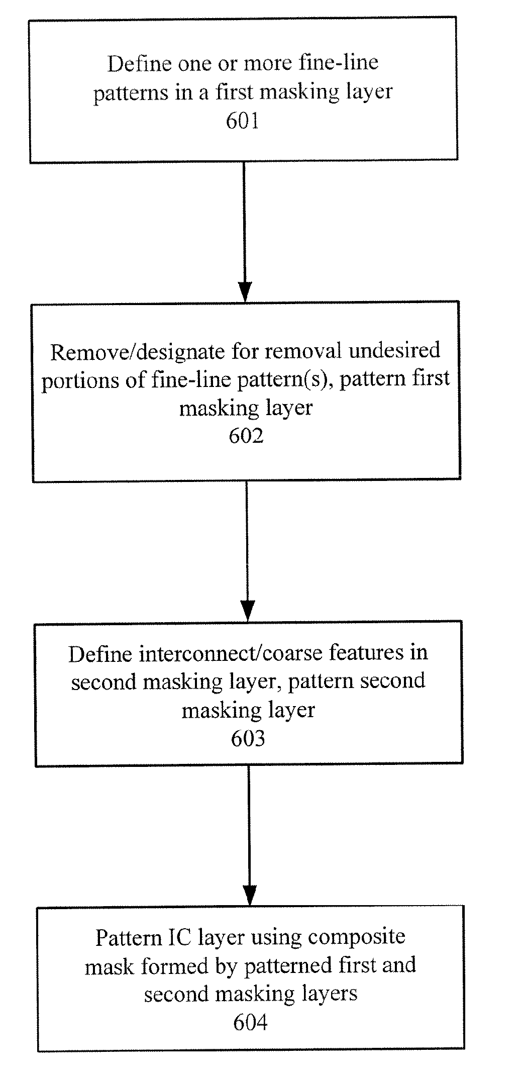
[0036]Notably, for each integrated circuit (IC) layer, many of the features can be characterized as having a periodic (or at least a quasi-periodic) pattern. This periodicity can be advantageously leveraged in simplifying the patterns transferred to multiple masking layers on the wafer. As discussed above, any bends or corners on a mask feature at sub-wavelength technology nodes can significantly deteriorate pattern fidelity on the wafer. Therefore, using a simplified pattern on a mask (or for any pattern transfer tool) can facilitate optimized resolution of the (quasi-)periodic pattern on the wafer.

[0037]For example, in one embodiment, a first mask can be used to define one or more geometrically regular fine-line patterns in a first masking layer on the surface of the wafer. Notably, each feature defined by the first mask is sub-wavelength i.e. its width is less than the wavelength of light used to form that feature, and therefore is called a fine-line feature herein.

[0038]FIG. 3A ...


PUM

PropertyMeasurementUnit
sizeaaaaaaaaaa
feature sizeaaaaaaaaaa
widthaaaaaaaaaa

Abstract

A multiple mask and a multiple masking layer technique can be used to pattern a single IC layer. A resolution enhancement technique can be used to define one or more fine-line patterns in a first masking layer, wherein each fine-line feature is sub-wavelength. Moreover, the pitch of each fine-line pattern is less than or equal to that wavelength. The portions of the fine-line features not needed to implement the circuit design are then removed or designated for removal using a mask. After patterning of the first masking layer, another mask can then be used to define coarse features in a second masking layer formed over the patterned first masking layer. At least one coarse feature is defined to connect two fine-line features. The IC layer can be patterned using the composite mask formed by the patterned first and second masking layers.

Description

BACKGROUND OF THE INVENTION[0001]1. Field of the Invention[0002]The present invention relates to forming features of an integrated circuit (IC) and in particular achieving sub-wavelength resolution of certain features in the IC in a cost-effective manner.[0003]2. Description of the Related Art[0004]In designing an integrated circuit (IC), engineers typically rely upon computer simulation tools to help create a schematic circuit design consisting of individual circuit elements electrically coupled together in order to perform certain functions. To actually fabricate this integrated circuit in a semiconductor substrate, the circuit design must be translated into a physical representation, or layout, which itself can then be transferred onto a series of templates (e.g. masks) used to sequentially pattern layers in or on the semiconductor substrate surface. Computer aided design (CAD) tools assist layout designers in the task of translating the circuit design into a series of two-dimens...

Claims


Application Information

Patent Timeline
Patent Type & Authority Applications(United States)
IPC IPC(8): G03F1/00G03C5/00G03B27/42
CPCG03F1/14H01L21/0337G03F7/70466G03F1/70
Inventor LIU, TSU-JAE KING
Owner SYNOPSYS INC
Why Eureka
Try Eureka