

Method for fabricating chip package
a chip and package technology, applied in the field of packaging, can solve the problems of affecting the quality of the product,
- Summary
- Abstract
- Description
- Claims
- Application Information
AI Technical Summary
Problems solved by technology
Method used
Image

Examples
embodiment 1
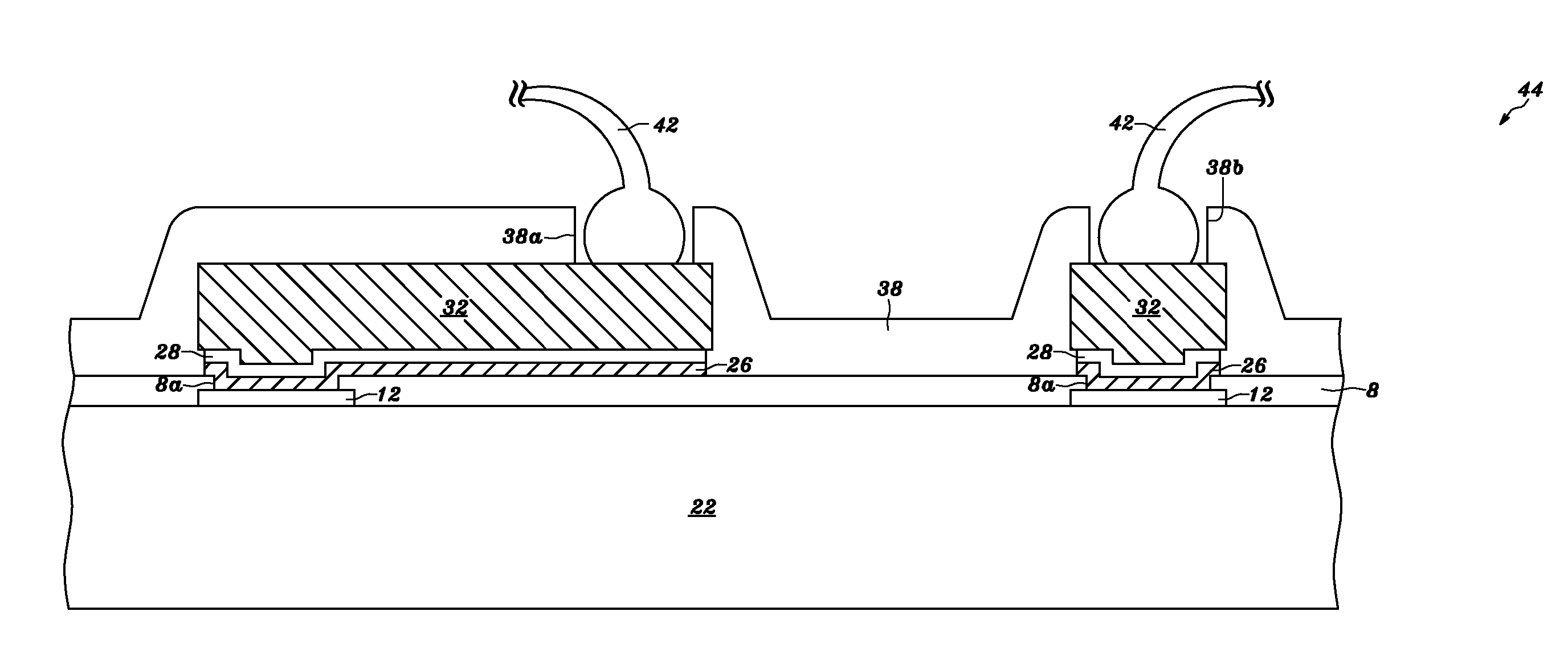
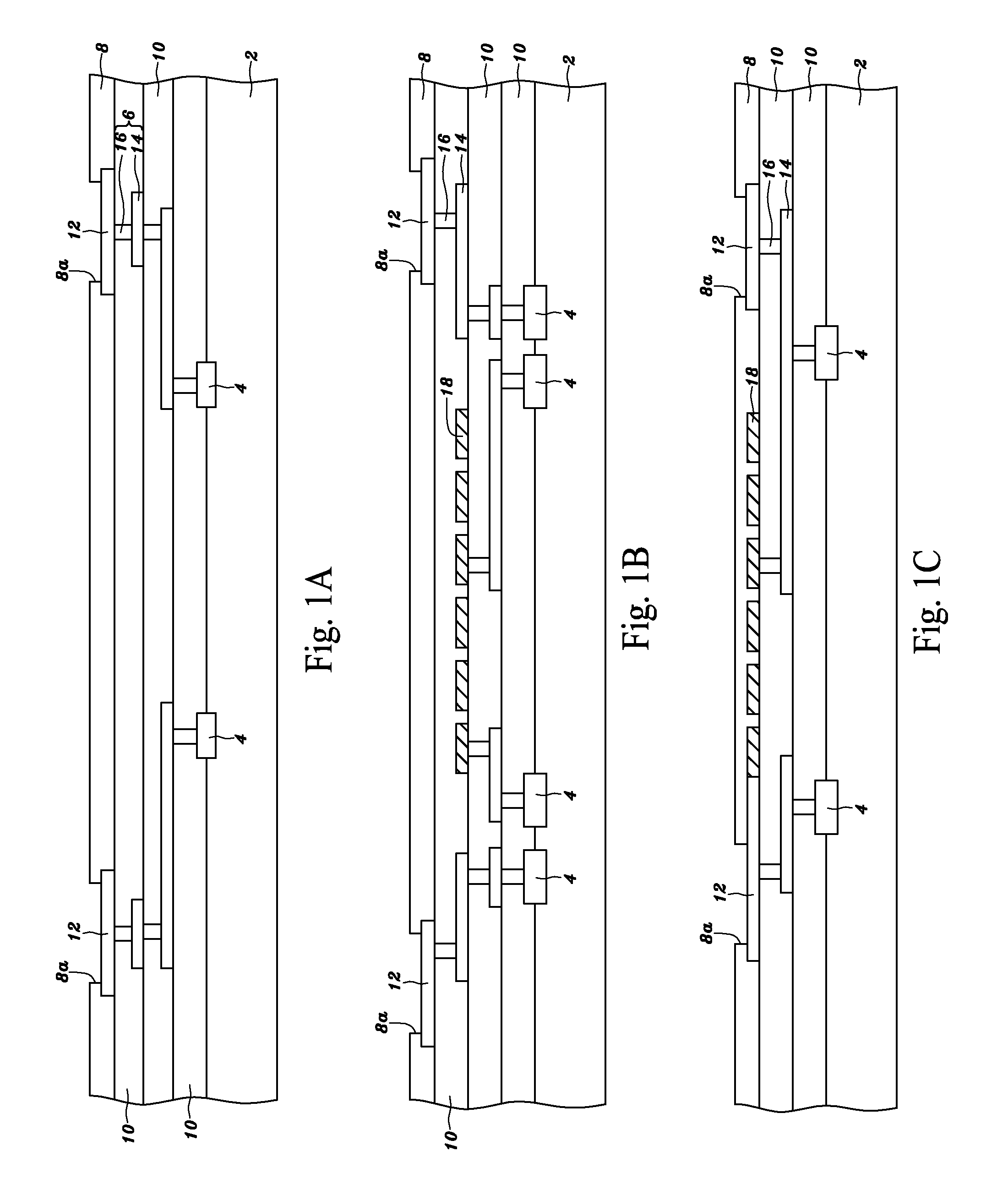
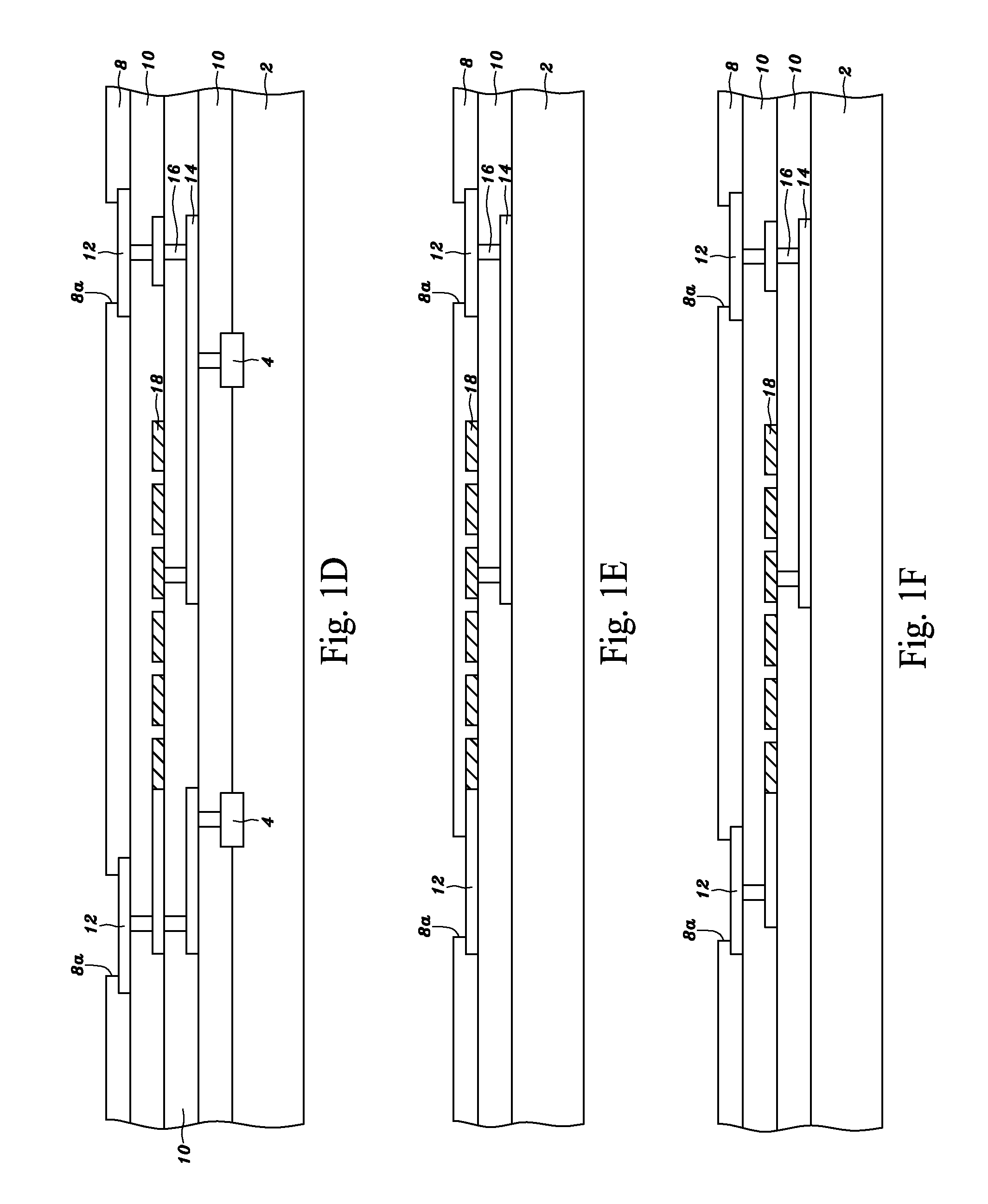
[0039] Referring to FIG. 2A, a polymer layer 24 is formed on the passivation layer 8 and two openings 24a are formed in the polymer layer 24 by patterning the polymer layer 24 to respectively expose two pads 12, as shown in FIG. 2B and FIG. 2C. The opening 24a may expose a portion of the pad 12, and another portion of the pad 12 is covered with the polymer layer 24, as shown in FIG. 2B. Alternatively, the opening 24a may expose the entire upper surface of the pad 12 exposed by the opening 8a in the passivation layer 8 and further may expose the upper surface of the passivation layer 8 near the pad 12, as shown in FIG. 2C. The descriptions of this embodiment in FIGS. 2D-2K are based on the structure with the opening 24a exposes a portion of the pad 12 and with another portion of the pad 12 covered by the polymer layer 24, as shown in FIG. 2B. Alternatively, the embodiments in FIGS. 2D-2K can be applied to the structure with the opening 24a exposes the entire upper surface of the pad ...
embodiment 2
[0067] Referring to FIG. 3A, after the step shown in FIG. 2E is completed, the photoresist layer 30 is patterned with the processes of exposure, development, etc., to form an opening 30c in the photoresist layer 30 exposing the seed layer 28 over the pads 12 and over the passivation layer 8.
[0068] The photoresist layer 30 can be formed by spin-on coating a positive-type photosensitive polymer layer having a thickness of between 5 and 30 μm, and preferably of between 7 and 15 μm, on the seed layer 28, then exposing the photosensitive polymer layer using a 1X stepper with at least two of G-line having a wavelength ranging from 434 to 438 nm, H-line having a wavelength ranging from 403 to 407 nm, and I-line having a wavelength ranging from 363 to 367 nm, illuminating the photosensitive polymer layer, that is, G-line and H-line, G-line and I-line, H-line and I-line, or G-line, H-line and I-line illuminate the photosensitive polymer layer, then developing the exposed polymer layer, and ...
embodiment 3
[0084] Referring to FIG. 2A, a polymer layer 24 is formed on the passivation layer 8, and then referring to FIGS. 4A-4B, at least one opening 24a is formed in the polymer layer 24 by patterning the polymer layer 24 to expose at least one pad 12. The opening 24a may expose a portion of the pad 12, and another portion of the pad 12 is covered with the polymer layer 24, as shown in FIG. 4A. Alternatively, the opening 24a may expose the entire upper surface of the pad 12 exposed by the opening 8a in the passivation layer 8 and further may expose the upper surface of the passivation layer 8 near the pad 12, as shown in FIG. 4B. The descriptions of this embodiment in FIGS. 4C-4L are based on the structure with the opening 24a exposes the entire upper surface of the pad 12 exposed by the opening 8a in the passivation layer 8 and further exposes the top surface of the passivation layer 8 in the perimeter of the pad 12, as shown in FIG. 4B. Alternatively, the embodiments in FIGS. 4C-4L can b...
PUM
| Property | Measurement | Unit |
|---|---|---|
| thickness | aaaaa | aaaaa |
| thickness | aaaaa | aaaaa |
| thickness | aaaaa | aaaaa |
Abstract
Description
Claims
Application Information