Semiconductor package having improved adhesion and solderability

a technology of soldering and sealing, applied in the direction of semiconductor devices, semiconductor/solid-state device details, electrical equipment, etc., can solve the problems of less metallization for good adhesion of known leadframes, more difficult to maintain mold compound adhesion to leadframes required to avoid device delamination, etc., to achieve enhanced down-bonding capability, improved moisture-level quality, and easy manufacturing

Inactive Publication Date: 2006-06-15
TEXAS INSTR INC
View PDF4 Cites 21 Cited by
  • Summary
  • Abstract
  • Description
  • Claims
  • Application Information

AI Technical Summary

Benefits of technology

[0023] It belongs to the technical advantages of the invention that no toxic or whiskering materials are used for the plating steps, down-bonding capability is enhanced, and m

Problems solved by technology

The recent general trend to avoid Pb in the electronics industry and use Pb-free solders, pushes the reflow temperature range into the neighborhood of about 260° C. This higher reflow temperature range makes it more difficult to maintain the mold compound adhesion

Method used


Image

  • Semiconductor package having improved adhesion and solderability
  • Semiconductor package having improved adhesion and solderability
  • Semiconductor package having improved adhesion and solderability

Examples


Embodiment Construction

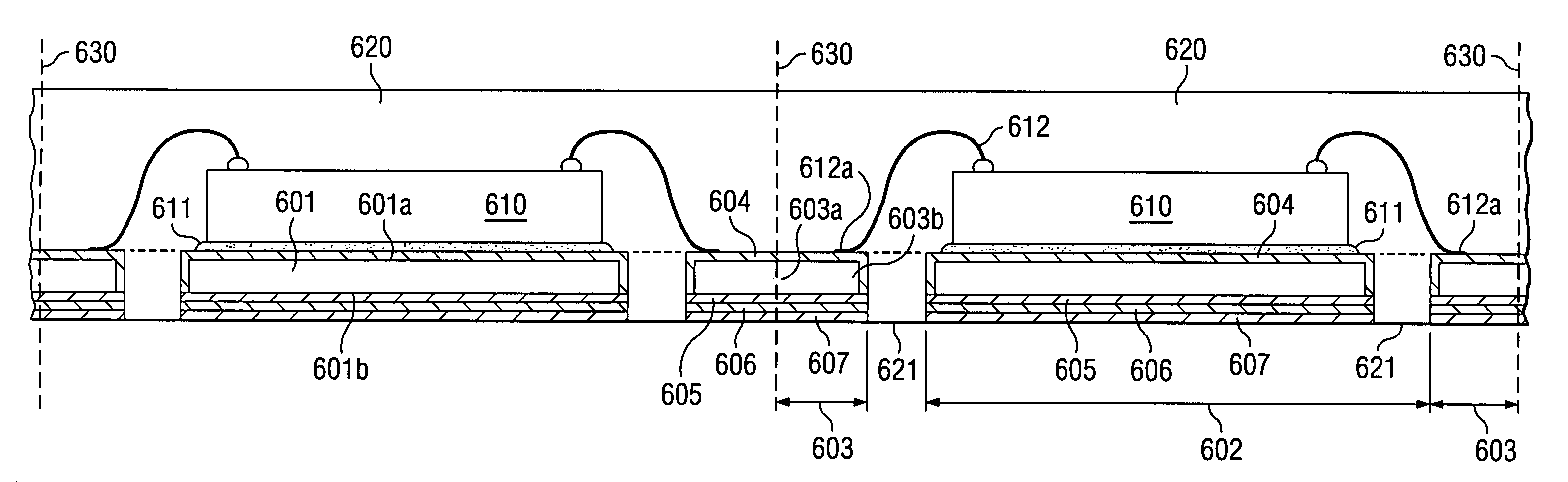
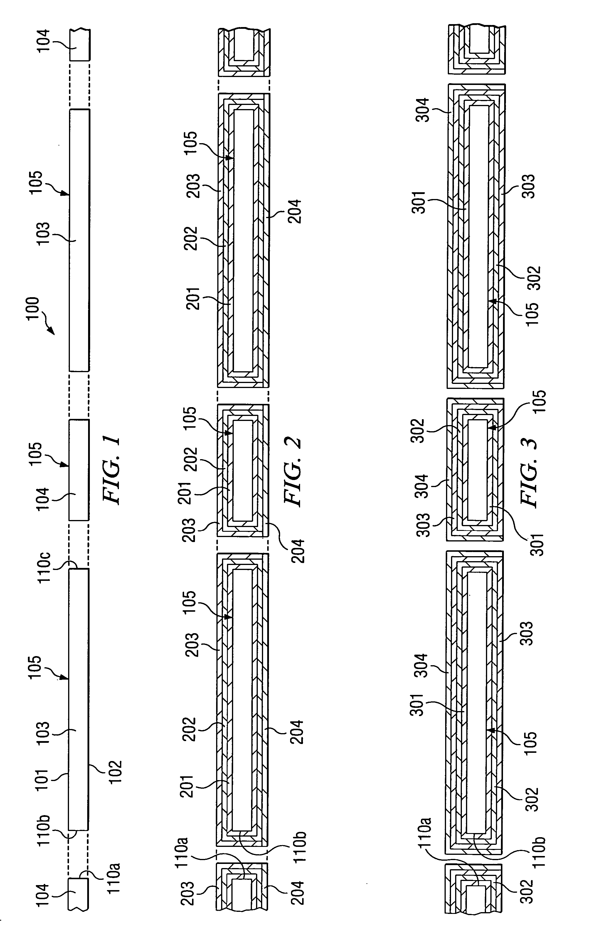
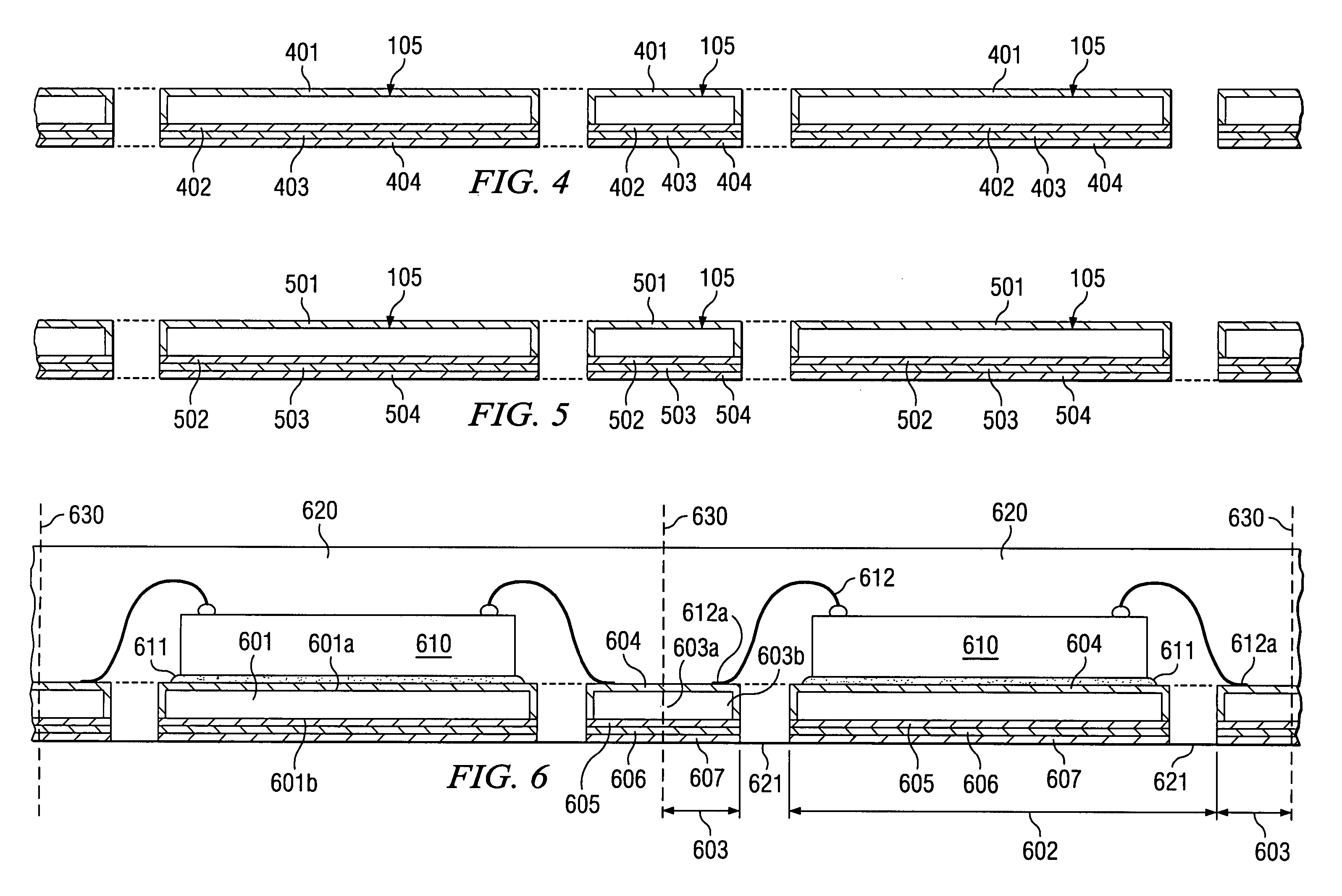
[0034]FIG. 1 is a schematic and simplified cross section of the starting material of a leadframe portion, generally designated 100. The leadframe has a first surface 101 and a second surface 102. The portion depicted contains a plurality of chip mount pads 103 and a plurality of lead segments 104. The leadframe is made of a base metal 105.

[0035] As defined herein, the starting material of the leadframe is called the “base metal”, indicating the type of metal. Consequently, the term “base metal” is not to be construed in an electrochemical sense (as in opposition to ‘noble metal’) or in a structural sense.

[0036] Base metal 105 is typically copper or a copper alloy. Other choices comprise brass, aluminum, iron-nickel alloys (“Alloy 42”), and covar.

[0037] Base metal 105 originates with a metal sheet in the preferred thickness range from 100 to 300 μm; thinner sheets are possible. The ductility in this thickness range provides the 5 to 15% elongation that facilitates the segment bend...


PUM


Abstract

A leadframe with a base metal structure (for example, copper) and first and second surfaces. A first metal layer, which is adhesive to polymeric materials such as molding compounds, is adherent to the first leadframe surface. The second leadframe surface is covered by a second metal layer for affinity to reflow metals such as tin alloy; this second metal layer has a different composition from the first metal layer. One example of the first surface is a nickel layer (201) in contact with the base metal (105), a palladium layer (202) in contact with the nickel layer, and an outermost tin layer (203) in contact with the palladium. Another example is an oxidized surface of the base metal. The second metal layer, on the second leadframe surface, comprises a nickel layer (201) in contact with the base metal (105), a palladium layer (202) in contact with the nickel layer, and an outermost gold layer (204) in contact with the palladium layer.

Description

FIELD OF THE INVENTION [0001] The present invention is related in general to the field of semiconductor devices and processes, and more specifically to the materials and fabrication of leadframes for integrated circuit devices and semiconductor components. DESCRIPTION OF THE RELATED ART [0002] Leadframes for semiconductor devices provide a stable support pad for firmly positioning the semiconductor chip, usually an integrated circuit (IC) chip within a package. Since the leadframe, including the pad, is made of electrically conductive material, the pad may be biased, when needed, to any electrical potential required by the network involving the semiconductor device, especially the ground potential. [0003] In addition, the leadframe offers a plurality of conductive segments to bring various electrical conductors into close proximity of the chip. The remaining gap between the inner end of the segments and the contact pads on the IC surface are bridged connectors, typically thin metall...

Claims


Application Information

Patent Timeline
IPC IPC(8): H01L23/495
CPCH01L23/3107H01L23/49582H01L24/48H01L24/97H01L2224/05599H01L2224/32245H01L2224/48091H01L2224/48247H01L2224/48465H01L2224/73265H01L2224/85439H01L2224/85444H01L2224/85464H01L2224/97H01L2924/01005H01L2924/01013H01L2924/01014H01L2924/01027H01L2924/01028H01L2924/01029H01L2924/01031H01L2924/01032H01L2924/01046H01L2924/01047H01L2924/01049H01L2924/0105H01L2924/01057H01L2924/01078H01L2924/01079H01L2924/01082H01L2924/01083H01L2924/01322H01L2924/014H01L2924/14H01L2924/00014H01L2224/85H01L2224/83H01L2924/01006H01L2924/01033H01L2224/45099H01L2924/00H01L2924/00012H01L2224/451
Inventor ZUNIGA-ORTIZ, EDGAR R.KODURI, SREENIVASAN K.ABBOTT, DONALD C.
Owner TEXAS INSTR INC
Why Eureka
Try Eureka