

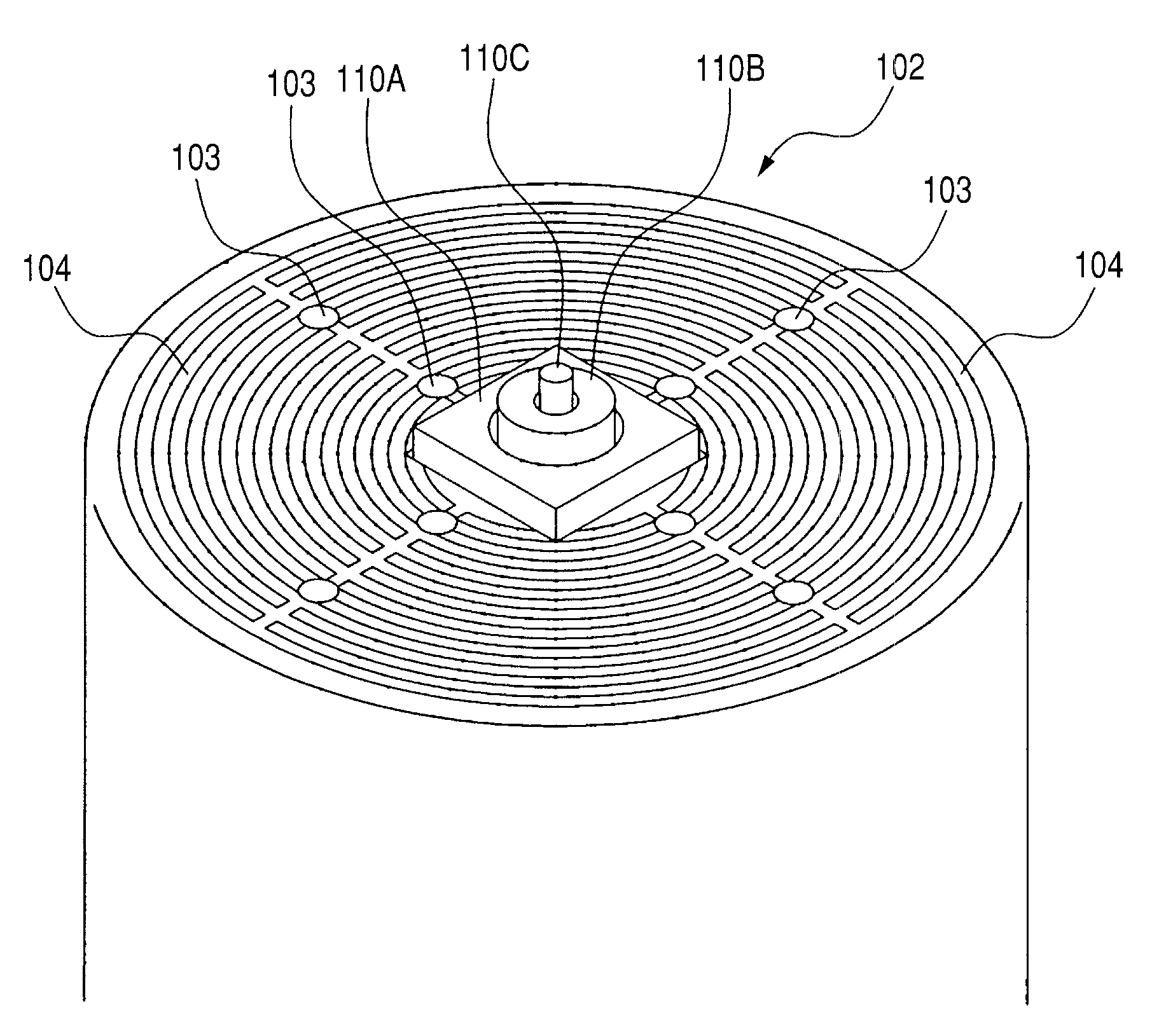
Fabrication method of semiconductor device
- Summary
- Abstract
- Description
- Claims
- Application Information
AI Technical Summary
Benefits of technology
Problems solved by technology
Method used
Image

Examples
first embodiment
[0126]In the first embodiment, the invention is applied to the fabrication of a semiconductor package in which a chip is mounted over a wiring substrate. Description will be given to the fabrication method in the order of process steps with reference to FIG. 1 to FIG. 33.
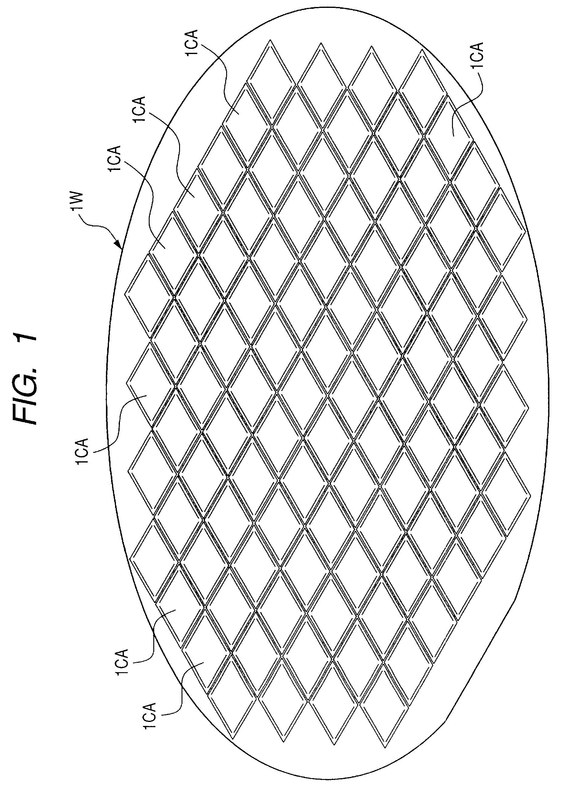
[0127]First, integrated circuits are formed in the principal surface of a wafer 1W formed of single crystal silicon illustrated in FIG. 1. Thereafter, the integrated circuit formed in each of the multiple chip formation areas (chip areas) 1CA partitioned by lattice-shaped scribe lines (parting areas) is subjected to an electrical test to determine its acceptability. The chip formation areas 1CA in the wafer 1W used in the first embodiment are in square planar shape with their longitudinal length equal to their lateral length.
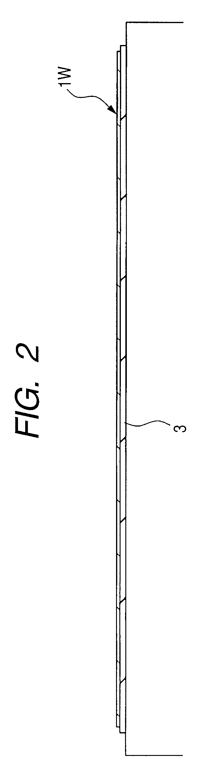
[0128]Next, as illustrated in FIG. 2, a back grind tape 3 for integrated circuit protection is stuck to the integrated circuit formation surface (on the lower side of the drawing) of the wafer 1...
second embodiment
[0169]In the second embodiment, the vacuum supply line described in relation to the first embodiment is constructed otherwise. (Refer to FIG. 29 and FIG. 30 for the vacuum supply line of the first embodiment.) The constructions of the other steps and members are the same as those in the first embodiment.
[0170]FIG. 34 is an explanatory drawing of a vacuum supply line for supplying reduced pressure to the vacuuming collet 105 in the second embodiment. Also, in the second embodiment, the vacuum supply line is formed of two systems. However, what is supplied through the pipe 122 is not a vacuum but air. The intensity of air supplied through the pipe (first air supply system) 122 is set so as to supply an appropriately smaller flow rate as compared with the pull-in flow rate on the vacuum side (the pipe 121) to control the vacuum pressure. When the vacuum pull-in flow rate of the pipe 121 is approximately 20 L (liters) / min, for example, air is supplied through the pipe 122 at approximate...
third embodiment
[0171]The third embodiment is so constructed that the thermocompression bonding step as the pellet bonding step for a chip 1C, described in relation to the first and second embodiments is divided into two stages: a temporary pressure bonding step for bonding only part of a chip 1C by thermocompression; and a proper pressure bonding step for bonding the whole of the chip 1C by thermocompression. This is the same with the pellet bonding step for the second chip 14.
[0172]FIG. 35 is a perspective view of a substantial part of a bonding stage KBS used at the above temporary pressure bonding step. FIG. 36 is a perspective view of a substantial part illustrating the way a wiring substrate 11 and chips 1C are placed over the bonding stage KBS.
[0173]The bonding stage KBS has protrusions TK on its surface opposed to the wiring substrate 11 and the chips 1C. FIG. 37 is a plan view illustrating in close-up a chip 1C placed over the bonding stage (first bonding stage) KBS. FIG. 38 is a sectional...
PUM
| Property | Measurement | Unit |
|---|---|---|
| Fraction | aaaaa | aaaaa |
| Thickness | aaaaa | aaaaa |
| Pressure | aaaaa | aaaaa |
Abstract
Description
Claims
Application Information