Compound semiconductor-on-silicon wafer with a thermally soft insulator

a technology of semiconductors and insulators, applied in the field of composite semiconductors on silicon wafers with thermally soft insulators, can solve the problems of high substrate cost, drive fabrication cost, and lattice mismatch between si and gan, and achieve the effect of avoiding wafer deformation

Inactive Publication Date: 2007-12-06
SHARP LAB OF AMERICA INC
View PDF4 Cites 14 Cited by
  • Summary
  • Abstract
  • Description
  • Claims
  • Application Information

AI Technical Summary

Benefits of technology

[0009]The present invention describes GaN grown on a Si wafer with a soft buried insulator to absorb the thermal mismatches. The structure is similar in concept to a buried oxide layer (BOX) of a Si-on-insulator (SOI) wafer. That is, the so-called “thermally soft insulator” (TSI) isolates mechanical stresses between the GaN layer and the Si substrate, avoiding wafer deformation. In one aspect, conventional boronphosphosilicate glass (BPSG) is used as the thermal insulator. At high wafer temperat

Problems solved by technology

However, these substrates are expensive to make, and their small size also drives fabrication costs.
There are two fundamental problems associated with GaN-on-Si device technology.
First, there is a lattice mismatch between Si and GaN.
However, an additional and more serious problem exists, as there is also a thermal mismatch between Si and GaN.
Although the lattice buffer layer may absorb p

Method used


Image

  • Compound semiconductor-on-silicon wafer with a thermally soft insulator
  • Compound semiconductor-on-silicon wafer with a thermally soft insulator
  • Compound semiconductor-on-silicon wafer with a thermally soft insulator

Examples


Embodiment Construction

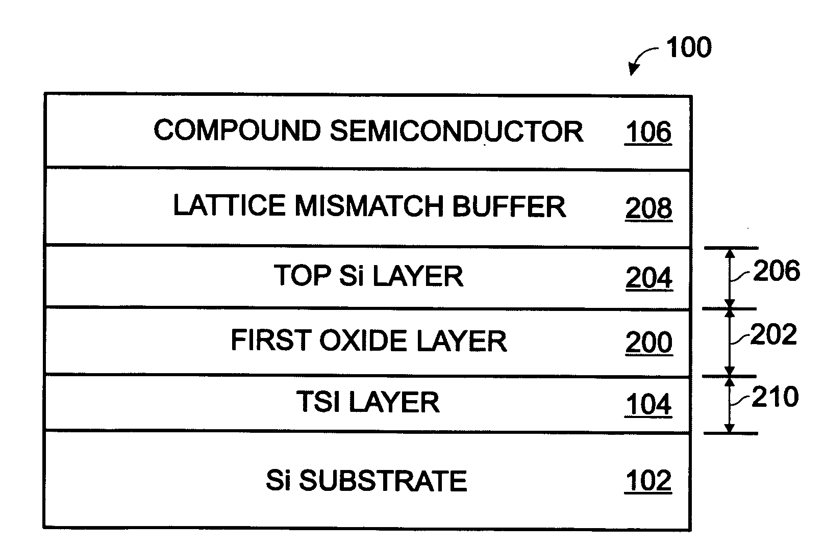
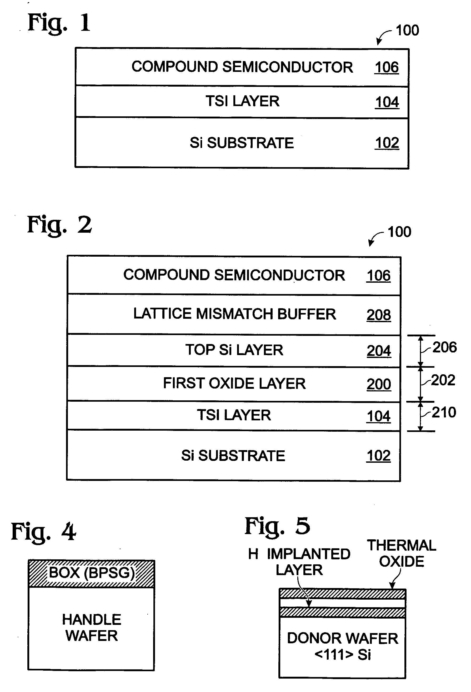
[0019]FIG. 1 is a partial cross-sectional view of a compound semiconductor-on-silicon (Si) wafer with a thermally soft insulator. In a simple aspect, the thermally soft insulated (TSI) wafer 100 comprises a Si substrate 102, a thermally soft insulator layer 104 overlying the Si substrate 102, and a compound semiconductor layer 106 overlying the thermally soft insulator layer 104. The thermally soft insulator 104 has a liquid phase temperature lower than the liquid phase temperatures of Si 102 or the compound semiconductor 106.

[0020]The thermally soft insulator (TSI) layer 104 has a flow temperature in the range of about 500° C. to 900° C., where the flow temperature is greater than the solid phase temperature and less than the liquid phase temperature. The TSI insulator layer 104 may be considered to be mechanically soft at the flow temperature, soft enough to isolate any differences in thermal expansion between the Si substrate 102 and the compound semiconductor 106. That is, the T...


PUM


Abstract

A method is provided for forming a compound semiconductor-on-silicon (Si) wafer with a thermally soft insulator. The method forms a Si substrate, with a thermally soft insulator layer overlying the Si substrate. A silicon oxide layer is formed immediately overlying the thermally soft insulator layer, a top Si layer overlies the silicon oxide, and a lattice mismatch buffer layer overlies the top Si layer. A compound semiconductor layer is formed overlying the lattice mismatch buffer layer. The thermally soft insulator has a liquid phase temperature lower than the liquid phase temperatures of Si and the compound semiconductor. For example, the thermally soft insulator may have a flow temperature in the range of about 500° C. to 900° C., where the flow temperature is greater than the solid phase temperature and less than the liquid phase temperature.

Description

BACKGROUND OF THE INVENTION[0001]1. Field of the Invention[0002]This invention generally relates to integrated circuit (IC) fabrication and, more particularly, to a wafer that uses a layer to insulate a compound semiconductor from thermally-induced lattice mismatches with an underlying silicon (Si) substrate.[0003]2. Description of the Related Art[0004]Gallium nitride (GaN) is a Group III / Group V compound semiconductor material with wide bandgap (3.4 eV), which has optoelectronic, as well as other applications. Like other Group III nitrides, GaN has a low sensitivity to ionizing radiation, and so, is useful in solar cells. GaN is also useful in the fabrication of blue light-emitting diodes (LEDs) and lasers. Unlike previous indirect bandgap devices (e.g., silicon carbide), GaN LEDs are bright enough for daylight applications. GaN devices also have application in high power and high frequency devices, such as power amplifiers.[0005]GaN LEDs are conventionally fabricated using a metal...

Claims


Application Information

Patent Timeline
IPC IPC(8): H01L27/12H01L21/84
CPCH01L21/02381H01L21/0245H01L21/02488H01L21/7624H01L21/02529H01L21/02538H01L21/02505
Inventor HSU, SHENG TENGLI, TINGKAILEE, JONG-JAN
Owner SHARP LAB OF AMERICA INC
Why Eureka
Try Eureka