Semiconductor integrated circuit devices having high-Q wafer back-side capacitors

a technology of integrated circuits and capacitors, which is applied in the direction of semiconductor devices, semiconductor/solid-state device details, electrical equipment, etc., can solve the problems of high power supply and ground noise, the use of on-chip capacitors is problematic, and the integration density is limited

Active Publication Date: 2007-12-06
GLOBALFOUNDRIES US INC
View PDF10 Cites 46 Cited by
  • Summary
  • Abstract
  • Description
  • Claims
  • Application Information

AI Technical Summary

Benefits of technology

[0058]It is to be appreciated that there are various advantages associated with exemplary methods of the invention for fabricating semiconductor devices with backside capacitor structures according to the invention. For instance, high-density integration can be achieved by forming the large area capacitors, if needed, on the chip back-side and thus, saving chip front-side area for more dense packaging of circuit components and interconnections. Moreover, back-side capacitors are disposed in relatively close relation to the front-side integrated circuit such that the length of interconnects (through wafer plug contacts) are minimized and thus minimizing the series resistance of the through-wafer interconnect structures.

Problems solved by technology

Insufficient decoupling capacitance can result in high power supply and ground noise.
Depending on the application, however, the use of on-chip capacitors can be problematic.
For example, with high-density chip designs, there can be limited 2D / 3D silicon space on the chip for building the integrated capacitors, resulting in practical limitations in integration density.
Consequently, to achieve a desired level of integration for a given design, the sizes of the on-chip capacitors may be reduced, resulting in decreased performance.
Moreover, the type of on-chip capacitor that is used in a given design may limit the level of performance and / or integration density achievable.
For example, high-performance chips are typically fabricated using capacitor technologies that yield high quality factor (Q) capacitors, but such technologies do not scale well as integration density increases, as higher integration results in formation of capacitors with relatively poor performance due to increased parasitic impedances and plate resistance.
Other capacitor technologies enable high-integration designs, but result in lower quality capacitors that are not useful in high-performance applications.
For instance, deep-trench or stacked capacitor techniques that are used in DRAM technology can be used to achieve high capacitance density, but can result in low quality capacitors.
For instance, with such technologies, the thin dielectric layers that are formed on capacitor trench sidewalls and 3D-structures can not sustain high-voltage stress and thus, susceptible to breakdown.
To address this problem, several capacitors must be serially connected to obtain an effective capacitance, but this technique results in four times increase in the area needed to construct the capacitors, and increase the cost of fabrication.
Other conventional techniques using planar or 3-D MIM (metal-insulation-metal) capacitor, interdigitated structure, etc., may be used to form high-quality capacitors, but at the expense of consuming valuable silicon real estate on the chip front side.

Method used


Image

  • Semiconductor integrated circuit devices having high-Q wafer back-side capacitors
  • Semiconductor integrated circuit devices having high-Q wafer back-side capacitors
  • Semiconductor integrated circuit devices having high-Q wafer back-side capacitors

Examples


Embodiment Construction

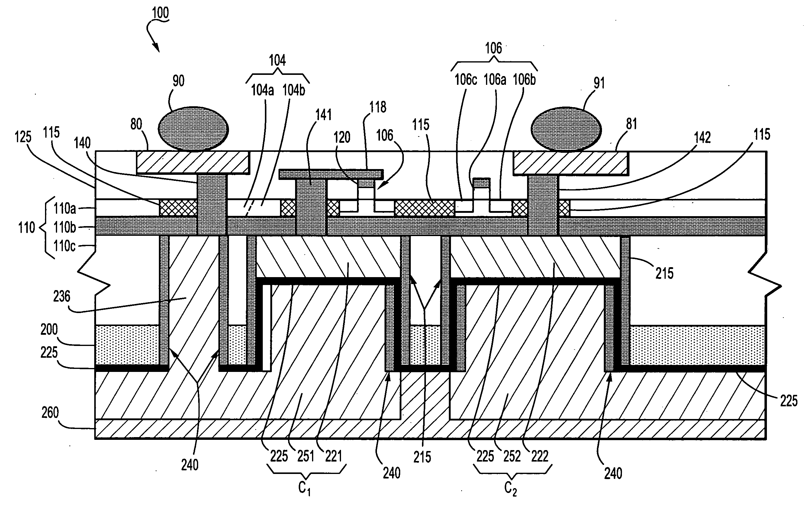
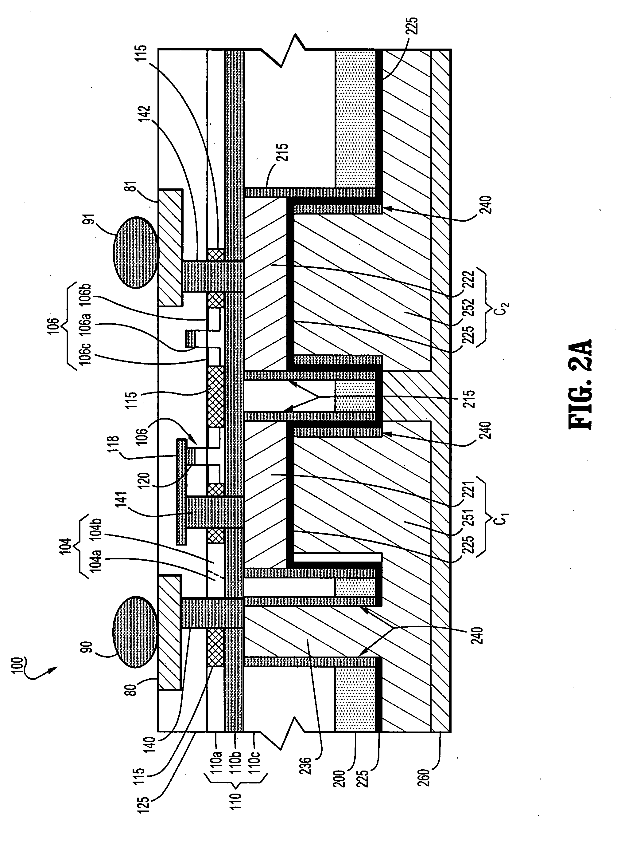
[0021]Exemplary embodiments of the invention will be discussed in further detail hereafter regarding semiconductor IC chips having high-quality, integrated capacitors that are fabricated on the chip back-side and connected to integrated circuits on the chip front-side using through-wafer interconnects. For example, exemplary chip fabrication techniques according to the invention as discussed below include methods for constructing large-size, high-quality capacitor structures on the back side of a semiconductor SOI (silicon-on-insulator) wafer while preserving the front side silicon real estate for achieving high density integration chip design. As discussed in detail below, exemplary chip fabrication techniques enable formation of high-quality capacitors with good dielectric integrity, low plate resistance and minimal or no parasitic impedances.

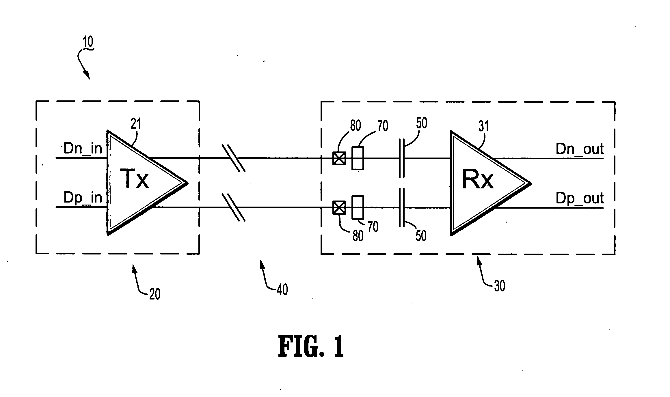
[0022]FIG. 1 schematically illustrates a Serializer-Deserializer (SerDes) module (10) having IC chips that can be fabricated with on-chip ca...


PUM


Abstract

Methods are provided for fabricating semiconductor IC (integrated circuit) chips having high-Q on-chip capacitors formed on the chip back-side and connected to integrated circuits on the chip front-side using through-wafer interconnects. In one aspect, a semiconductor device includes a semiconductor substrate having a front side, a back side, and a buried insulating layer interposed between the front and back sides of the substrate. An integrated circuit is formed on the front side of the semiconductor substrate, an integrated capacitor is formed on the back side of the semiconductor substrate, and an interconnection structure is formed through the buried insulating layer to connect the integrated capacitor to the integrated circuit.

Description

TECHNICAL FIELD OF THE INVENTION [0001]The present invention relates generally to methods for fabricating semiconductor IC (integrated circuit) chips having high-Q on-chip capacitors and, more specifically, semiconductor IC chips having high-Q capacitors that are formed on the chip back-side and connected to integrated circuits on the chip front-side using through-wafer embedded interconnects.BACKGROUND [0002]In general, capacitors are components that are commonly used in chip fabrication and packaging designs for various purposes. For instance, on-chip capacitors are fundamental components for constructing semiconductor integrated circuits including, for example, memory arrays, charge pumps, RC filters, peaking amplifiers and various types of analog integrated circuits. In addition, capacitors are used in integrated circuits and chip packages for purposes of AC coupling and DC blocking. For example, capacitors can be implemented as series elements that couple RF energy from one par...

Claims


Application Information

Patent Timeline
Patent Type & Authority Applications(United States)
IPC IPC(8): H01L29/00
CPCH01L21/76898H01L21/84H01L23/5223H01L27/1203Y10S438/957H01L2924/0002H01L23/481H01L2924/00
Inventor CLEVENGER, LAWRENCEDALTON, TIMOTHY JOSEPHHSU, LOUISRADENS, CARLRAMACHANDRAN, VIDHYAWONG, KEITH KWONG HONYANG, CHIH-CHAO
Owner GLOBALFOUNDRIES US INC
Why Eureka
Try Eureka