Method of fabricating circuit board having different electrical connection structures

a technology of electrical connection structure and circuit board, which is applied in the direction of sustainable manufacturing/processing, final product manufacturing, non-metallic protective coating application, etc., can solve the problems of electrical connection with a chip or a printed circuit board, difficulty in controlling the height of the solder joint during reflow, and accompanying stencil printing of solder joints

Active Publication Date: 2007-12-06
PHOENIX PRECISION TECH CORP
View PDF1 Cites 11 Cited by
  • Summary
  • Abstract
  • Description
  • Claims
  • Application Information

AI Technical Summary

Benefits of technology

[0011]Another objective of the present invention is to provide a method of fabricating a circuit board having different electrical connecting structures, that are free from short circuit problems.
[0014]The formation of the metal adhesive layer on the first and the second conductive pads is achieved by sputtering, evaporation, or electroless plating (chemical deposition), and the formation of the metal posts on the second conductive pads is made by electroplating. Therefore, the pitch between adjacent first electrical connection structures, adjacent second electrical connection structures or adjacent first and second electrical connection structures, is allowed to be smaller than 160 μm. It makes the circuit board of the present invention a fine pitch solution that can meet the requirement for the high-performance electronic products. Further, as the metal posts are formed by methods other than stencil printing, the height of the metal posts can be satisfactorily controlled such that electrical connection problems existing in the prior art can thus be eliminated.

Problems solved by technology

However, forming solder joints by stencil printing is accompanied by difficulty in the control of the height of the solder joints during reflow.
In consequence, the reflowed solder joints tend to be not equal in height, and thus their electrical connection with a chip or a printed circuit board is adversely affected.
Moreover, the formation of the solder joints by stencil by printing the solder material on the conductive pads of the circuit board body is difficult in the control of the amount of the solder material.
It thus easily results in the occurrence of a bridging phenomenon between adjacent solder joints and a short circuit problem will accordingly take place.
In other words, solder joints formed by conventional printing methods fail to be fine-pitched, such that there is always a limitation in the application of the current flip chip semiconductor packages.
Accordingly, a critical issue to circuit board manufacturers nowadays involves solving the above drawbacks and meeting the requirements of mechanical and electrical characteristics for solder joints concurrently.

Method used


Image

  • Method of fabricating circuit board having different electrical connection structures
  • Method of fabricating circuit board having different electrical connection structures
  • Method of fabricating circuit board having different electrical connection structures

Examples


Embodiment Construction

[0020]The following illustrative embodiments are provided to illustrate the disclosure of the present invention, these and other advantages and effects can be apparently understood by those in the art after reading the disclosure of this specification. The present invention can also be performed or applied by other different embodiments. The details of the specification may be on the basis of different points and applications, and numerous modifications and variations can be devised without departing from the spirit of the present invention.

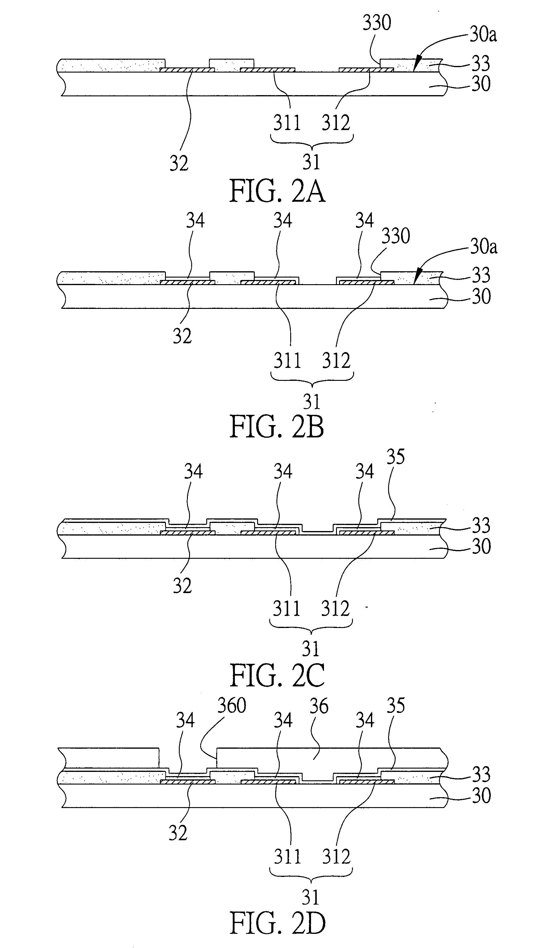
[0021]Referring to FIGS. 2A to 2G, steps for the method of fabricating a circuit board having different electrical connection structures of the present invention are shown.

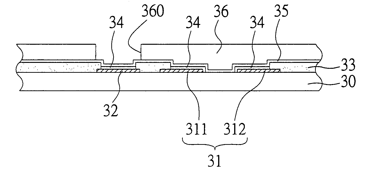
[0022]As shown in FIG. 2A, a bi-layered or multi-layered circuit board body 30 is provided. A plurality of first conductive pads 31, a plurality of second conductive pads 32 and a solder masks layer 33 are formed on a surface 30a of the circuit board body 30.

[0023]The first con...


PUM


Abstract

A method of fabricating an electrical connecting structure of a circuit board is disclosed. The method includes: providing a circuit board having a plurality of first and a plurality of second conductive pads; forming on the circuit board a solder mask having a plurality of openings to thereby expose the first and the second conductive pads; forming an metal adhesive layer on the first and the second conductive pads; forming a conductive layer on the circuit board and the metal adhesive layer; forming on the conductive layer a resistive layer, wherein a plurality of openings are formed in the resistive layer to expose the conductive layer on the second conductive pads; forming a metal post by electroplating through the conductive layer on the second conductive pads; removing the resistive layer and the conductive layer covered underneath; and forming a soldering layer on the metal post. This invention discloses a method of forming different connecting elements on a circuit board.

Description

BACKGROUND OF THE INVENTION[0001]1. Field of the Invention[0002]This invention relates to methods of fabricating a circuit board, and more particularly, to a method of fabricating a circuit board having a plurality of electrical connection structures.[0003]2. Description of Related Art[0004]With the rapid development in technology, electronic products are capable of being made in a compact size, performed with multiple functions, and operated at a high speed. Therefore, packaging industry has been thriving to come up with advanced or improved semiconductor packages in order to meet the need for high performance electronic products.[0005]A flip chip semiconductor package is one of the most advanced semiconductor packages in the art. The flip chip semiconductor package typically features in forming a plurality of solder bumps on electrode pads formed on an active surface of a semiconductor chip, such that the semiconductor chip can be electrically connected to a packaging substrate by...

Claims


Application Information

Patent Timeline
Patent Type & Authority Applications(United States)
IPC IPC(8): H01R4/02
CPCH01L21/4846H01L21/4853H01L2924/0002H01L23/49838H05K1/111H05K3/243H05K3/28H05K2201/0367H05K2201/0391H05K2201/09381H05K2201/09436H05K2201/10636H01L2224/05027H01L2224/05018H01L2224/05559H01L2224/13006H01L2224/05572H01L2224/0401H01L2224/05552H01L2224/13562Y02P70/50
Inventor SHIH, CHAO-WEN
Owner PHOENIX PRECISION TECH CORP
Why Eureka
Try Eureka