
Semiconductor apparatus and method of disposing observation flip-flop

a technology of semiconductor apparatus and flip-flop, which is applied in the direction of fluid pressure measurement, testing circuit, instruments, etc., can solve the problems of reducing the current supply capacity of elements that form an internal circuit, operating power supply voltage, and inability to keep track of the state of signal lines in internal circuits through external terminals of semiconductor apparatus. , to achieve the effect of shortening the distance between the observation flip-flop and the signal line, suppressing the increase of signal lines, and avoiding an increas

Inactive Publication Date: 2007-12-06
RENESAS ELECTRONICS CORP
View PDF11 Cites 3 Cited by
  • Summary
  • Abstract
  • Description
  • Claims
  • Application Information

AI Technical Summary

Benefits of technology

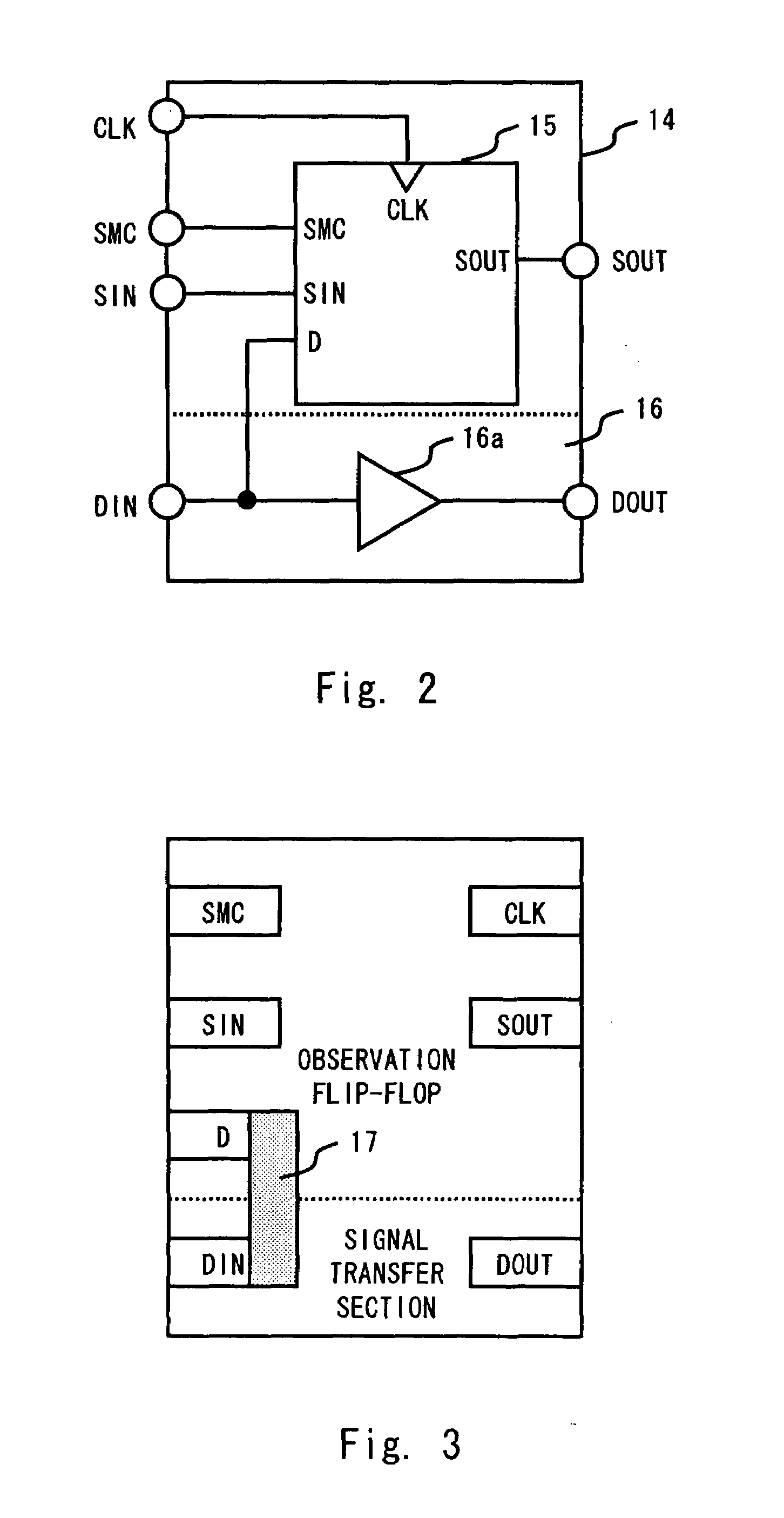
The present invention provides a semiconductor apparatus and a method of disposing an observation flip-flop to observe the state of a signal line. The technical effect of this invention is that it reduces parasitic capacitance of a line from the signal line to the observation flip-flop, which prevents an increase in signal delay and malfunction of the semiconductor apparatus. This is achieved by placing the observation flip-flop as a functional block including a signal transfer section and an observation flip-flop, and connecting the signal line through the signal transfer section. Additionally, the method of disposing an observation flip-flop includes placing the signal transfer section and the observation flip-flop in the same functional block, which further reduces the distance between them.

Problems solved by technology

However, as a circuit size increases, a connection of signal lines in an internal circuit becomes complex, which makes it unable to keep track of the state of signal lines in an internal circuit through an external terminal of the semiconductor apparatus.
A decrease in operating power supply voltage generally leads to a decrease in current supply capacity of elements that form an internal circuit.
If large capacitance is connected to the output of those elements in such a condition, the delay of an output signal increases.
In short, the placement of an observation flip-flop, which is added to improve the reliability of a semiconductor apparatus, causes an increase in parasitic capacitance of a signal line, which leads to an increase in signal delay in an internal circuit.
This can cause malfunction of the semiconductor apparatus.

Method used


Image

  • Semiconductor apparatus and method of disposing observation flip-flop
  • Semiconductor apparatus and method of disposing observation flip-flop
  • Semiconductor apparatus and method of disposing observation flip-flop

Examples


first embodiment

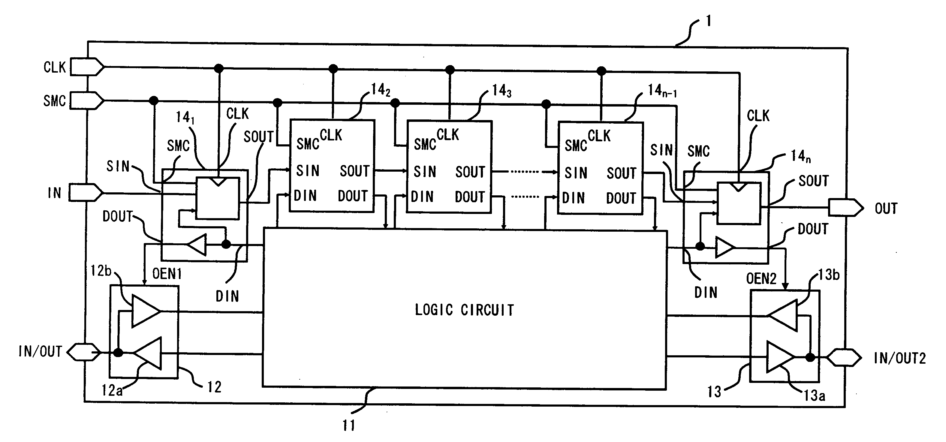
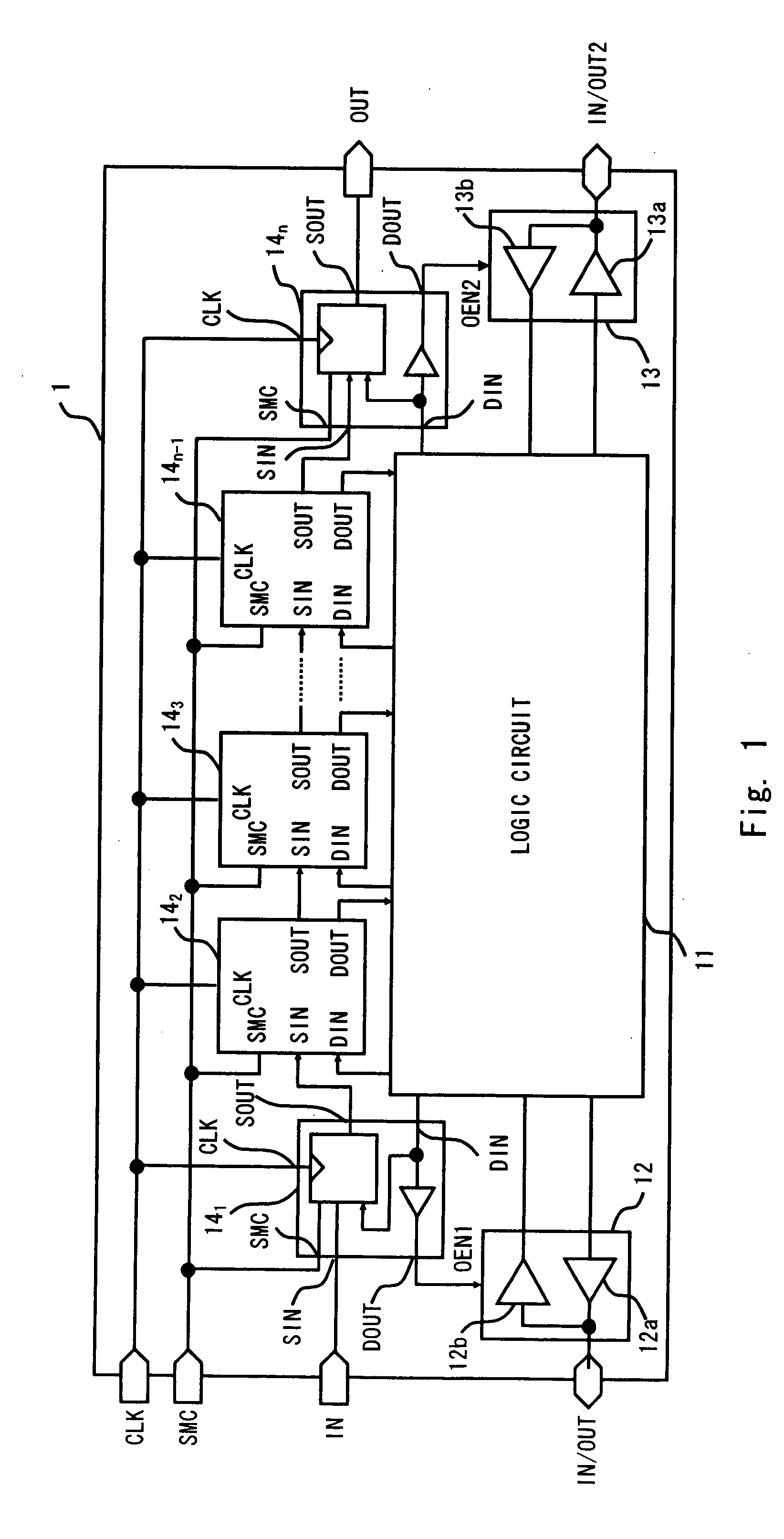
[0022]Exemplary embodiments of the present invention are described hereinafter with reference to the drawings. FIG. 1 is a block diagram of a semiconductor apparatus 1 according to a first embodiment of the present invention. As shown in FIG. 1, the semiconductor apparatus 1 includes a logic circuit 11, input / output buffers 12 and 13, and functional blocks 141 to 14n.

[0023]The logic circuit 1 serves as an information processing unit of the semiconductor apparatus 1, and functional circuits to be used by a user are formed in the logic circuit 1. The input / output buffer 12 includes an output buffer 12a and an input buffer 12b, and the input / output buffer 13 includes an output buffer 13a and an input buffer 13b. The input / output buffers 12 and 13 are buffer circuits capable of switching between an input mode and an output mode according to a switch signal OEN. In normal operation mode, the semiconductor apparatus 1 uses these blocks to exchange data with the outside and processes the e...

second embodiment

[0042]A semiconductor apparatus according to a second embodiment of the present invention is substantially the same as the semiconductor apparatus according to the first embodiment. However, the first embodiment and the second embodiment are different in the way of inserting a functional block. In the first embodiment, a scan chain circuit which uses a functional block is generated in the process of inserting a DFT circuit. In the second embodiment, on the other hand, a functional block is used only in a predetermined position.

[0043]FIG. 6 is a flowchart showing a design flow of the semiconductor apparatus according to the second embodiment. As shown in FIG. 6, the design flow of the second embodiment also begins with the RTL design (Step S1). Then, logic synthesis is performed on the basis of the description of the RTL design (Step S2′). In the second embodiment, a dummy buffer is inserted in Step S2′ into a signal line which, according to verification in the design phase, does not...


PUM


Abstract

A semiconductor apparatus includes a functional block to observe a state of a signal line in the apparatus. The functional block includes a signal transfer section to receive, transmit and output the state of the signal line, and an observation flip-flop to store a state of an input terminal or an output terminal of the signal transfer section.

Description

BACKGROUND OF THE INVENTION[0001]1. Field of the Invention[0002]The present invention relates to a semiconductor apparatus and a method of disposing an observation flip-flop. Particularly, the present invention relates to a semiconductor apparatus and a method of disposing an observation flip-flop which suppress an increase in line capacitance due to the addition of an observation flip-flop.[0003]2. Description of Related Art[0004]A circuit of a semiconductor apparatus is recently increasing in size. A semiconductor apparatus usually undergoes a short-circuit test of a signal line in the apparatus. However, as a circuit size increases, a connection of signal lines in an internal circuit becomes complex, which makes it unable to keep track of the state of signal lines in an internal circuit through an external terminal of the semiconductor apparatus. To address this, recent semiconductor apparatus employ a scan chain circuit, which is composed of observation flip-flops connected in s...

Claims


Application Information

Patent Timeline
Patent Type & Authority Applications(United States)
IPC IPC(8): G01R31/28
CPCG01R31/318583
Inventor HAYASHI, MASAHIKO
Owner RENESAS ELECTRONICS CORP
Learn More