Liquid crystal display device and semiconductor device

a liquid crystal display and semiconductor technology, applied in semiconductor devices, instruments, electrical apparatus, etc., can solve the problems of insufficient size and direction of electric field applied to liquid crystal molecules, insufficient arrangement interval and width of opening patterns of pixel electrodes, and decreased current drive capability of transistors, so as to improve the degree of freedom of intervals between

Inactive Publication Date: 2007-12-13
SEMICON ENERGY LAB CO LTD
View PDF26 Cites 134 Cited by
  • Summary
  • Abstract
  • Description
  • Claims
  • Application Information

AI Technical Summary

Benefits of technology

[0048]By employing the invention, an interval between the first electrode and the second electrode can be increased and controlled without affecting another element, so that degree of freedom of the interval therebetween is improved. Accordingly, since optimal values for an arrangement interval and width of an opening pattern of a pixel electrode change depending on a distance between the pixel electrode and a common electrode, the size, the width, and the interval of the opening pattern c

Problems solved by technology

Therefore, even when a distance between the electrodes is made to be increased, there has been limitation.
If the thickness of the insulating film interposed between electrodes is increased, for example, since a gate insulating film in a transistor is thickened there is an adverse effect such that current drive capability of the transisto

Method used


Image

  • Liquid crystal display device and semiconductor device
  • Liquid crystal display device and semiconductor device
  • Liquid crystal display device and semiconductor device

Examples


embodiment mode 1

[0089]FIG. 37 is a cross-sectional view showing a basic structure of the invention. A first electrode 3701 is formed over a substrate 3700. The substrate 3700 is a glass substrate, a quartz substrate, a substrate formed of an insulator such as alumina, a plastic substrate having heat resistance which can resist processing temperature of a post-process, a silicon substrate, or a metal substrate. In the case of operating as a transmissive display device, it is preferable that the substrate 3700 have a light-transmitting property.

[0090]The first electrode 3701 is formed by using a conductive film which transmits visible light (e.g., ITO: Indium Tin Oxide).

[0091]An insulating film 3704 is formed over the substrate 3700 and the first electrode 3701. The insulating film 3704 is formed of an insulating substance having oxygen or nitrogen such as silicon oxide (SiOx), silicon nitride (SiNx), silicon oxynitride (SiOxNy: x>y), or silicon nitride oxide (SiNxOy: x>y), and may be a single-layer ...

embodiment mode 2

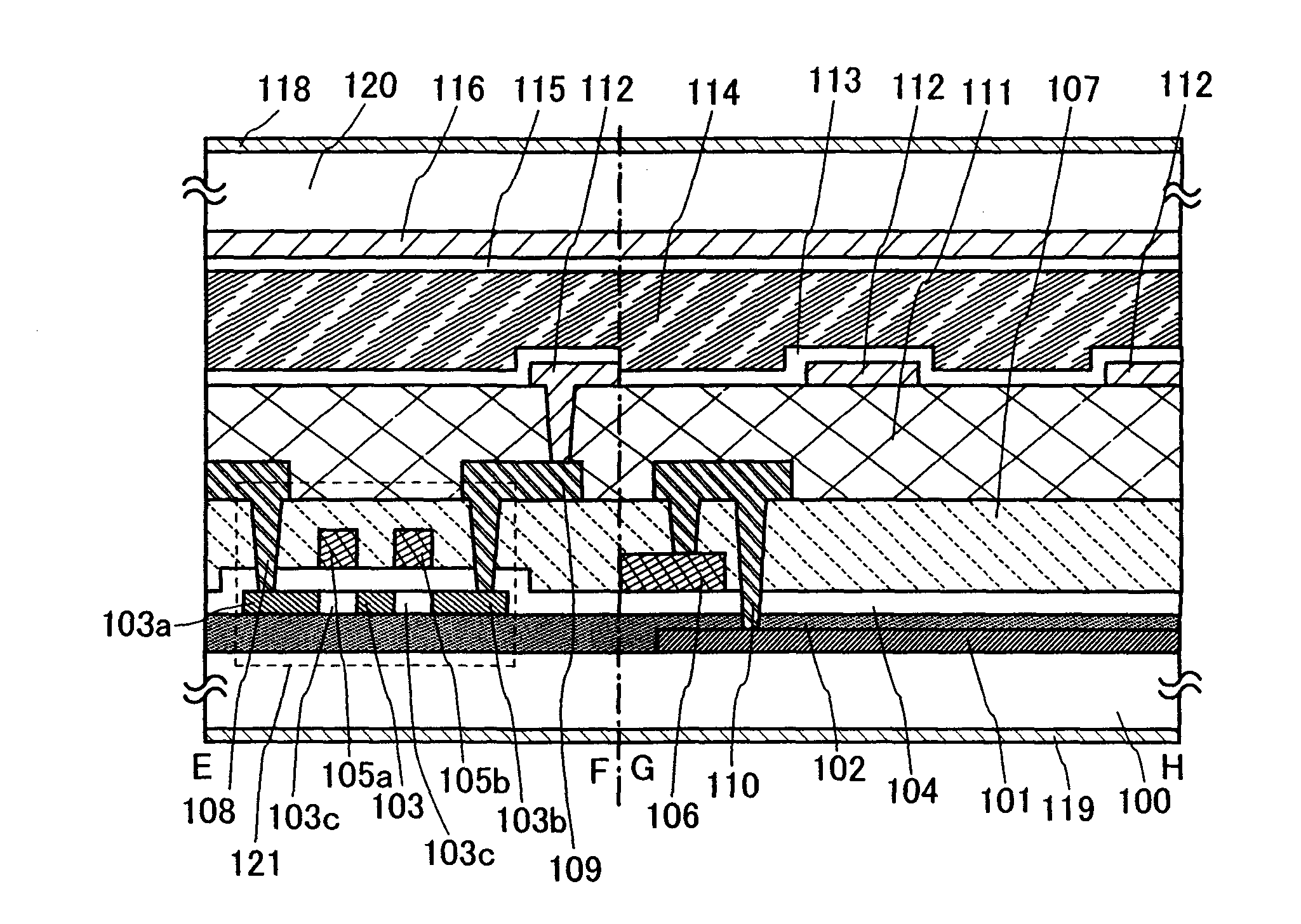
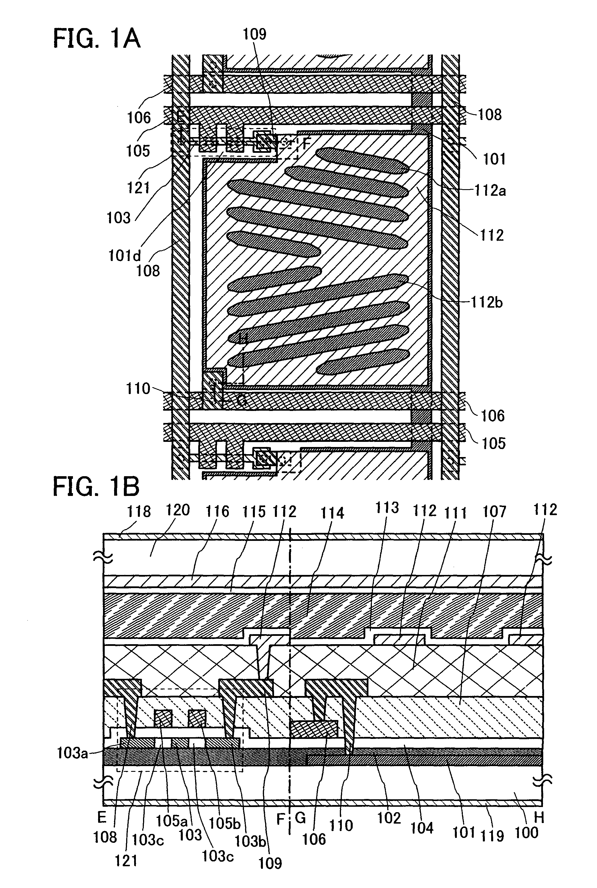
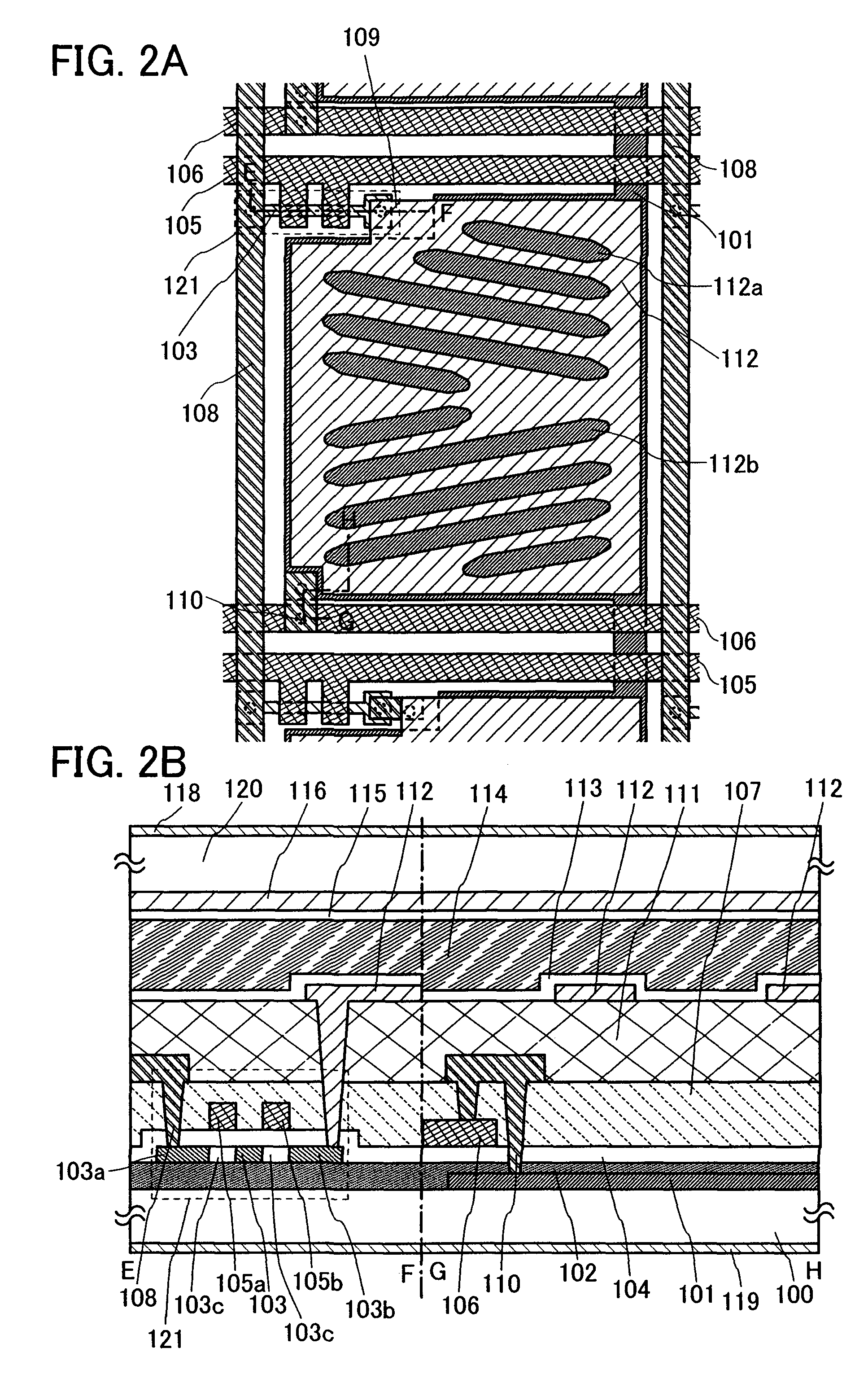
[0106]FIG. 1A is a plan view showing a structure of a liquid crystal display device in accordance with Embodiment Mode 2 of the invention. A pixel for one pixel is shown. This liquid crystal display device is a device which controls an alignment direction of liquid crystals by an FFS-mode. In FIG. 1A, a plurality of source wirings 108 are provided in parallel with each other (extended in a longitudinal direction in the drawing) and separated from each other. A plurality of gate wirings 105 are provided so as to be extended in a direction which is almost perpendicular to the source wirings 108 (in a horizontal direction in the drawing) and separated from each other. Auxiliary wirings 106 are provided in positions adjacent to each of the plurality of gate wirings 105, and extended in a direction which is almost parallel to the gate wirings 105, that is, in a direction which is almost perpendicular to the source wirings 108 (in the horizontal direction in the drawing). Almost rectangul...

embodiment mode 3

[0162]FIG. 3A is a plan view showing a structure of a liquid crystal display device in accordance with Embodiment Mode 3. FIG. 3B is a cross-sectional view taken along a line E-F and a line G-H in FIG. 3A. This embodiment mode describes a structure which is almost similar to that of Embodiment Mode 2 except for the following points. The first electrode 101 is electrically connected to the impurity region 103b of the thin film transistor 121 and functions as a pixel electrode; the second electrode 112 is electrically connected to the auxiliary wiring 106 and functions as a common electrode; the second electrode 112 protrudes outside of the first electrode 101 when seen from a direction which is perpendicular to the substrate 100; and connection structures of the first electrode 101 and the second electrode 112 to each wiring are different. In addition, a manufacturing method of the liquid crystal display device in accordance with this embodiment mode is almost similar to that of Embo...


PUM


Abstract

By increasing an interval between electrodes which drives liquid crystals, a gradient of an electric field applied between the electrodes can be controlled and an optimal electric field can be applied between the electrodes. The invention includes a first electrode formed over a substrate, an insulating film formed over the substrate and the first electrode, a thin film transistor including a semiconductor film in which a source, a channel region, and a drain are formed over the insulating film, a second electrode located over the semiconductor film and the first electrode and including first opening patterns, and liquid crystals provided over the second electrode.

Description

BACKGROUND OF THE INVENTION[0001]1. Field of the Invention[0002]The present invention relates to a semiconductor device and a liquid crystal display device. In particular, the invention relates to a semiconductor device and a liquid crystal display device each controlling liquid crystal molecules by generating an electric field almost parallel to a substrate.[0003]2. Description of the Related Art[0004]One of technical development strategies of a liquid crystal display device is widening a viewing angle. As a technique for realizing a wide viewing angle, a mode has been used in which gray scales are controlled by generating an electric field almost parallel to a substrate to move liquid crystal molecules within a surface parallel to the substrate. IPS (In-Plane Switching) and FFS (Fringe-Field Switching) are given as such a mode. In an FFS mode, a second electrode having an opening pattern (e.g., a pixel electrode of which a voltage is controlled per pixel) is provided below liquid ...

Claims


Application Information

Patent Timeline
IPC IPC(8): H01L31/112H01L29/80H01L31/0288
CPCG02F1/134363G02F1/136227G02F1/136286G02F1/136G02F1/1368G02F1/1337G02F1/134309G02F1/136277G02F1/133345G02F1/134372G02F2201/121G02F1/133707G02F1/13685G02F1/134318G02F1/13439
Inventor KIMURA, HAJIME
Owner SEMICON ENERGY LAB CO LTD
Why Eureka
Try Eureka