Dielectric memory and manufacturing method thereof

Active Publication Date: 2007-12-13
PANNOVA SEMIC
View PDF6 Cites 3 Cited by
  • Summary
  • Abstract
  • Description
  • Claims
  • Application Information

AI Technical Summary

Benefits of technology

[0023]The single elementary film of a noble metal is not reduced in the presence of hydrogen. Therefore, according to this method, the oxygen diffusi

Problems solved by technology

This leads to a problem that stress due to a thermal anneal easily causes a crack 522.
Therefore, defects such as deterioration of c

Method used


Image

  • Dielectric memory and manufacturing method thereof
  • Dielectric memory and manufacturing method thereof
  • Dielectric memory and manufacturing method thereof

Examples


embodiment 1

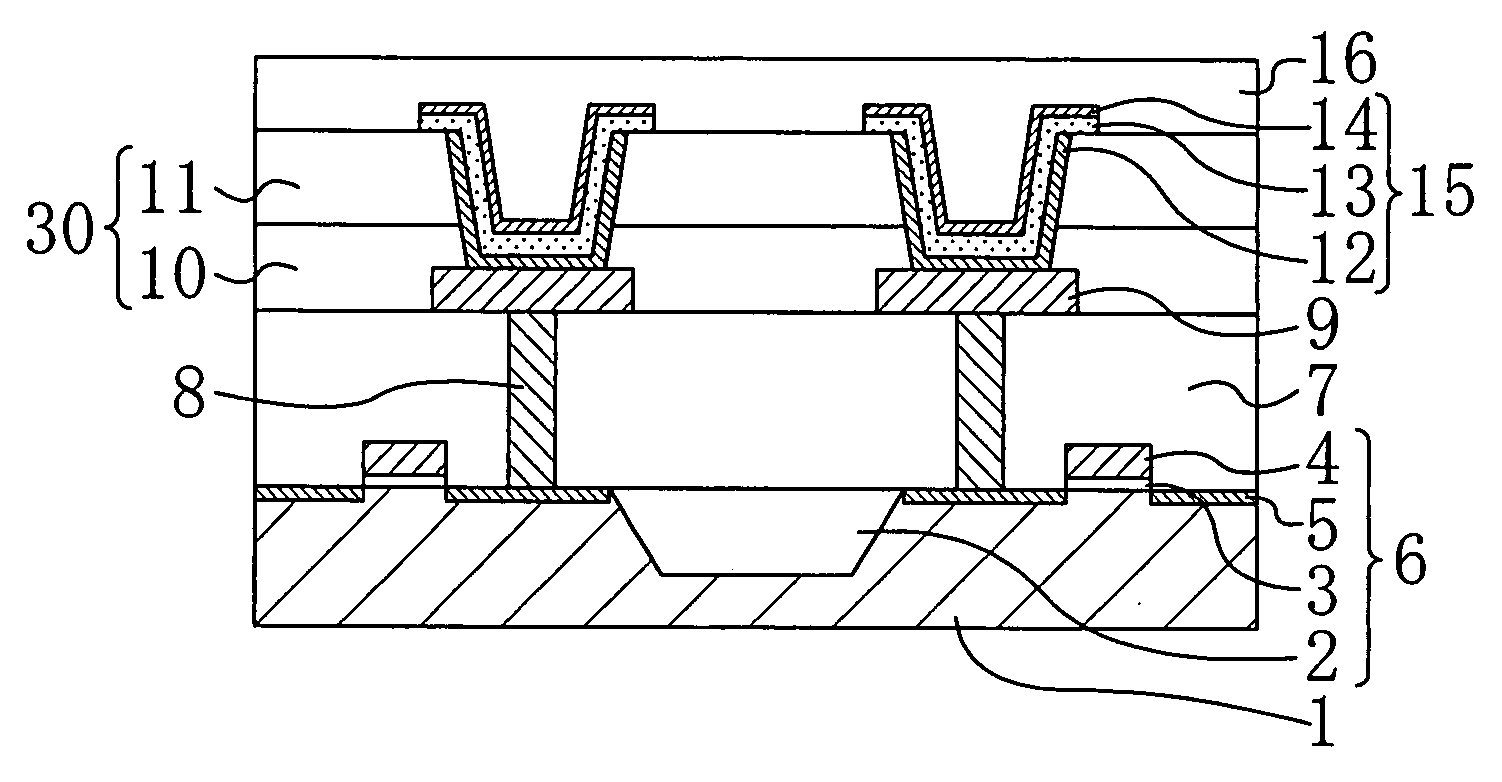
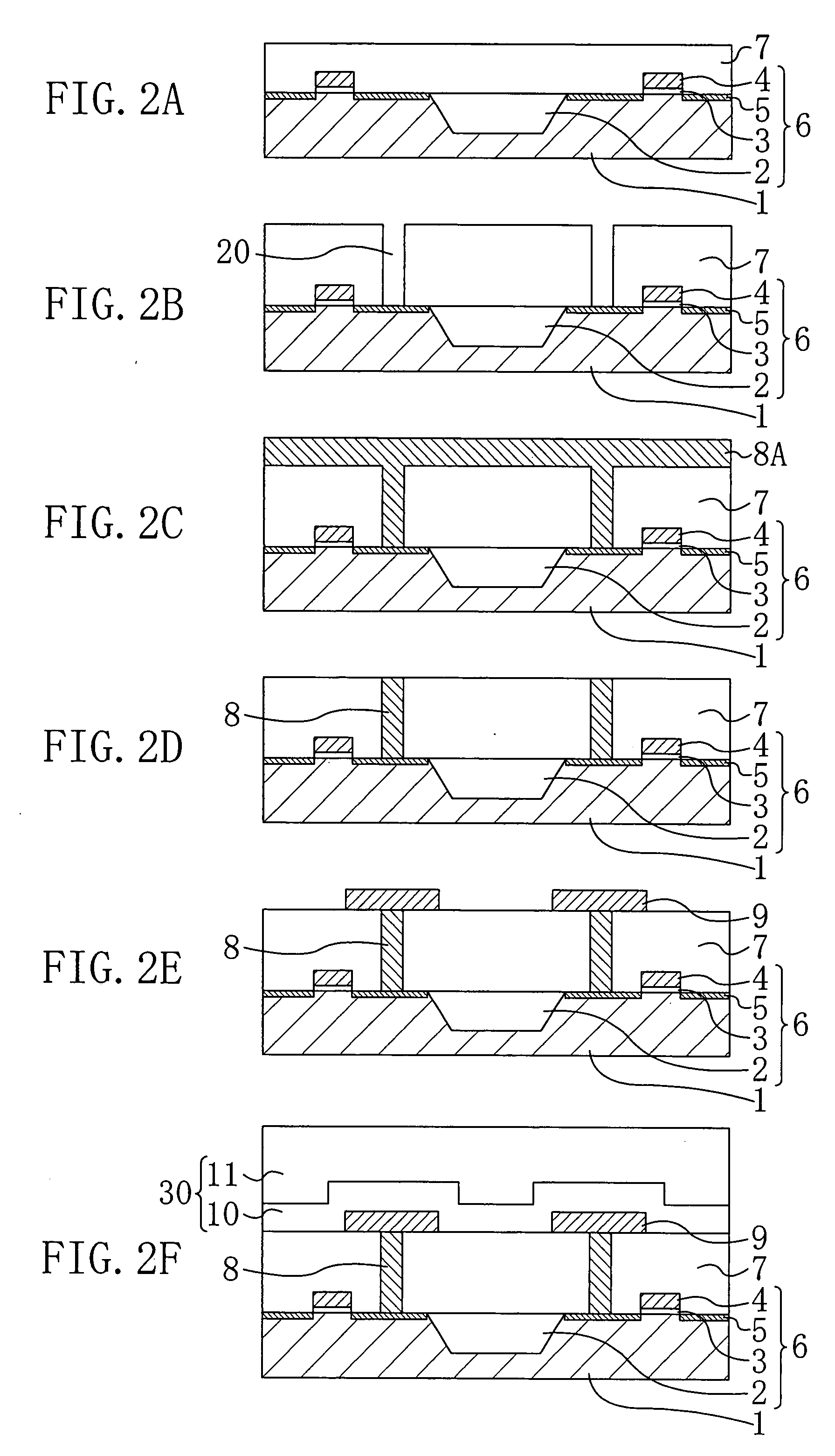
[0035]FIG. 1 is a cross section illustrating a structure of a dielectric memory according to Embodiment 1 of the present invention.

[0036]As shown in FIG. 1, a shallow trench isolation (STI) region 2 is provided in an upper part of a semiconductor substrate 1 which is formed of, for example, silicon (Si). Element formation regions are sectioned by the STI region 2. A transistor 6 is provided in each element formation region. The transistor 6 includes a gate insulation film 3 on the element formation region, a gate electrode 4 on the gate insulation film 3, and impurity diffusion layers 5 formed laterally on both sides of the gate electrode 4.

[0037]A first interlayer insulation film 7 formed of a silicon oxide is provided on the semiconductor substrate 1 to cover each transistor 6, the first interlayer insulation film 7 having a film thickness of about 0.4 μm to about 0.8 μm. An upper surface of the first interlayer insulation film 7 is flat. In this case, as the silicon oxide, a so-c...

embodiment 2

[0075]Embodiment 2 of the present invention will be described below with reference to the drawings. Note that, descriptions corresponding to Embodiment 1 are omitted.

[0076]As described above, as the oxygen diffusion prevention layer, a multilayer film formed of a metal nitride film and a single elementary film of a noble metal is used. That is, the oxygen diffusion prevention layer includes the single elementary film of a noble metal which is not reduced by hydrogen. Therefore, a plasma CVD oxide film which produces hydrogen can be directly formed on the oxygen diffusion prevention layer. Specifically, barrier function of oxygen diffusion prevention layer against oxygen is not decreased. Moreover, cracks in a thick ozone TEOS film can be eliminated because the ozone TEOS film is not used. Therefore, it is possible to suppress oxidation of a contact plug and improve reliability of the dielectric memory more than Embodiment 1.

[0077]A manufacturing method of a second dielectric memory ...


PUM


Abstract

As an oxygen diffusion prevention layer, a multilayer film formed by a metal nitride and a noble metal element. As an interlayer insulation film on the oxygen diffusion prevention layer, a plasma CVD oxide film is used. Moreover, as an interlayer insulation film on a capacitor, an ozone TEOS film is used.

Description

BACKGROUND OF THE INVENTION[0001]1. Field of the Invention[0002]The present invention relates to a dielectric memory including a vertically stacked capacitor having a high dielectric constant material or a ferroelectric material and to a manufacturing method of such dielectric memory.[0003]2. Description of the Prior Art[0004]In a semiconductor memory having a high dielectric constant material or a ferroelectric material, for large-scale integration, a stacked memory cell is employed instead of a conventional planar memory cell. In such semiconductor memory, a thermal anneal is performed at a high temperature in an oxygen atmosphere in order to crystallize a dielectric film, which is a metal oxide. The thermal anneal oxidizes a contact plug provided under a capacitor. In order to prevent the oxidation of the contact plug in such semiconductor memory, an oxygen diffusion prevention layer is provided on the contact plug (see, for example, Japanese Patent No. 3681632 or Japanese Laid-O...

Claims


Application Information

Patent Timeline
IPC IPC(8): H01L27/108H01L21/8242
CPCH01L27/11502H01L28/75H01L28/55H01L27/11507H10B53/30H10B53/00
Inventor NATSUME, SHINYA
Owner PANNOVA SEMIC
Why Eureka
Try Eureka