Heat dissipating structure and method for fabricating the same

a technology of heat dissipation structure and semiconductor chip, which is applied in the direction of semiconductor/solid-state device details, semiconductor devices, electrical apparatus, etc., can solve the problems of large amount of heat produced by the active surface the difficulty of efficiently dissipating the heat to the exterior, and the impact of the electric performance of the semiconductor chip and the product stability, so as to prevent the cracking of the semiconductor chip, reduce the cost of cutting, and avoid the effect of the chip crack

Inactive Publication Date: 2007-12-27
SILICONWARE PRECISION IND CO LTD
View PDF0 Cites 28 Cited by
  • Summary
  • Abstract
  • Description
  • Claims
  • Application Information

AI Technical Summary

Benefits of technology

[0023] Therefore, the heat sink package structure and method for fabricating the same mainly mounting and electrically connecting a semiconductor chip to a chip carrier; mounting an interface layer or a second heat dissipating element having an interface layer on the semiconductor chip; disposing a first heat dissipating element having a heat dissipating portion and a supporting portion on the chip carrier, wherein the heat dissipating portion has an opening formed corresponding to the semiconductor chip; forming an encapsulant that encapsulates the semiconductor chip, the interface layer or the second heat dissipating element having the interface layer, and the first heat dissipating element, wherein a height is reserved on top of the interface layer for the formation of the encapsulant for covering the interface layer, thereby preventing cracking of the semiconductor chip during the molding process; subsequently, cutting the encapsulant along edges of the interface layer or the heat dissipating element having the interface layer; and removing the encapsulant located on the interface layer, wherein, the interface layer can be removed together with the encapsulant located on the interface layer or left on. Thus, a heat sink package structure is formed without using the conventional grinding method, thereby avoiding the cracking of the semiconductor chip in grinding the encapsulant of the prior art. Meanwhile, since the cutting line does not pass through the heat dissipating element, the burr problem and wearing of cutting tools can be prevented and accordingly the cutting cost can be reduced.

Problems solved by technology

Such packages in operation produce a large amount of heat.
Otherwise, electric performance of semiconductor chips and product stability can be seriously affected.
As the encapsulants are generally made of a material having low heat conductivity such as only 0.8 w / m-° K., heat generated from active surfaces of semiconductor chips are difficult to be efficiently dissipated to the exterior, thereby adversely affecting electric performance and lifetime of the semiconductor chips.
If heat dissipating elements inside semiconductor packages are completely encapsulated by encapsulants, the heat dissipating path still needs to pass through the encapsulant and the heat dissipating efficiency is limited.
However, some drawbacks exist in fabricating the semiconductor package 10.
However, it is difficult to precisely control the mounting height of the semiconductor chip 11 to the substrate 12 so as to make the top surface of the semiconductor chip 11 precisely abut against the top wall of the mold cavity 15.
As a result, the overflow of the encapsulant is formed on the top surface of the semiconductor chip 11, which adversely affects the heat dissipating efficiency of the semiconductor chip 11 and the product appearance.
As a result, a deflash process is needed for removing the overflow of the encapsulant on the top surface of the semiconductor chip 11, which not only increases the fabrication time and the fabrication cost, but also may lead to product damage.
However, the grinding method needs a high cost.
In addition, warpage of the semiconductor package can occur due to a mismatch of coefficient of thermal expansion between the encapsulant and the heat sink or semiconductor chip, thus increasing difficulty of efficiently exposing surface of the semiconductor chip.
Also, the grinding forces may cause cracking of the semiconductor chip.
However, during the above cutting process, cutting tools need to pass through the heat dissipating elements.
As the heat dissipating elements are generally made of a metal material such as copper and aluminum, when a diamond cutting tool passes through the heat dissipating elements, rough edges or burrs can be formed on periphery of the heat dissipating elements, thereby adversely affecting the product appearance and causing wearing of the cutting tool.

Method used


Image

  • Heat dissipating structure and method for fabricating the same
  • Heat dissipating structure and method for fabricating the same
  • Heat dissipating structure and method for fabricating the same

Examples


first embodiment

[0037]FIGS. 5A to 5F are diagrams showing a heat sink package structure and method for fabricating the same according to a first embodiment of the present invention.

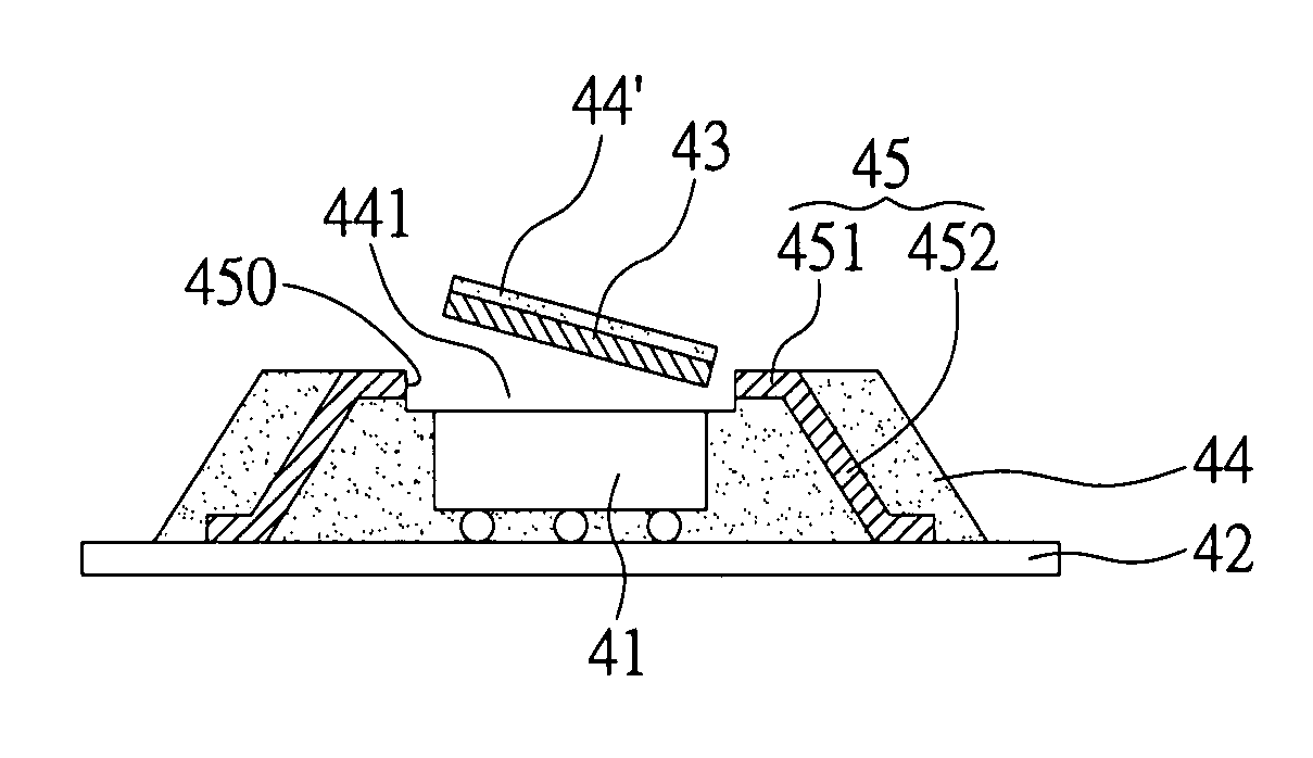
[0038] As shown in FIG. 5A, a semiconductor chip 41 is mounted to and electrically connected to a chip carrier 42 through one surface thereof, and an interface layer 43 is formed on the other surface of the semiconductor chip 41.

[0039] The chip carrier 42 may be a BGA substrate or an LGA substrate. The semiconductor chip 41 may be such as a flip-chip semiconductor chip, the active surface of which is electrically connected to the chip carrier 42 through a plurality of conductive bumps 410.

[0040] The interface layer 43 may be a P.I. tape adhered to the semiconductor chip 41, or an epoxy resin coated on semiconductor chip 41, or an organic layer made of such as wax formed on the semiconductor chip 41. Thus, the adhesion between the interface layer 43 and the encapsulant to be formed subsequently for encapsulating the se...

second embodiment

[0046]FIGS. 6A and 6B are sectional diagrams of a heat sink package structure according to a second embodiment of the present invention. In the present embodiment, an external heat slug 56 is disposed on the exposed surface of the semiconductor chip 51. As shown in FIG. 6A, the external heat slug 56 has shape of a flat plate. In addition, as shown in FIG. 6B, a plurality of fins can be formed on the external heat slug 56 for improving heat dissipating efficiency.

third embodiment

[0047]FIG. 7 is a sectional diagram showing a heat sink package structure according to a third embodiment of the present invention. In the present embodiment, a wire-bonding semiconductor chip 61 is mounted to a chip carrier 62 through its non-active surface, and electrically connected with the chip carrier 62 through a plurality of bonding wires 67. A material layer 68 such as a scraped chip or a heat dissipating element is mounted on the active surface of the semiconductor chip 61. Further, an interface layer (not shown) is mounted on the material layer 68. Thus, after the first heat dissipating element 65 is disposed on the chip carrier 62 and the molding process is performed, both the interface layer and the encapsulant on the interface layer can be removed so as to form a recess structure 641 for exposing the material layer 68 from the encapsulant 64, thereby increasing heat dissipating efficiency of the semiconductor chip 61.

[0048] It should be noted that the material layer 6...


PUM


Abstract

A heat sink package structure and a method for fabricating the same are disclosed. The method includes mounting and electrically connecting a semiconductor chip to a chip carrier, forming an interface layer or a second heat dissipating element having the interface layer on the semiconductor chip and installing a first heat dissipating element having a heat dissipating portion and a supporting portion onto the chip carrier. The method further includes forming openings corresponding to the semiconductor chip in the heat dissipating portion, and forming an encapsulant for covering the semiconductor chip, the interface layer or the second heat dissipating element, and the first heat dissipating element. A height is reserved on top of the interface layer for the formation of the encapsulant for covering the interface layer. The method further includes cutting the encapsulant along edges of the interface layer, and removing the redundant encapsulant on the interface layer. Therefore, the drawbacks of the prior art of the burrs caused by a cutting tool for cutting the heat dissipating element and wearing of the cutting tool are overcome.

Description

BACKGROUND OF THE INVENTION [0001] 1. Field of the Invention [0002] The present invention relates generally to semiconductor package structures and method for fabricating the same, and more particularly to heat sink semiconductor package structures that can efficiently dissipate heat produced by semiconductor chips and method for fabricating the same. [0003] 2. Description of Related Art [0004] Along with demands for lighter, thinner, smaller and shorter electronic products, semiconductor chip packages integrating high-density electronic components and electronic circuits have become a mainstream. Such packages in operation produce a large amount of heat. The heat must be dissipated timely. Otherwise, electric performance of semiconductor chips and product stability can be seriously affected. On the other hand, in order to protect internal circuits of semiconductor packages from mist and dust pollution, semiconductor chip surfaces are generally covered by encapsulants. As the encaps...

Claims


Application Information

Patent Timeline
Patent Type & Authority Applications(United States)
IPC IPC(8): H01L23/34H01L21/58
CPCH01L23/3121H01L23/4334H01L2224/4824H01L2924/01079H01L2924/1815H01L24/48H01L2924/01019H01L2224/73204H01L2924/18165H01L2924/00014H01L2224/45099H01L2224/45015H01L2924/207
Inventor HUANG, CHIEN-PINGPU, HAN-PINGTSAI, HO-YI
Owner SILICONWARE PRECISION IND CO LTD
Why Eureka
Try Eureka