Method to process polycrystalline lead selenide infrared detectors

a polycrystalline lead selenide and infrared detector technology, applied in the direction of photovoltaic energy generation, instruments, electrical equipment, etc., can solve the problems of poor yield, lack of reproducibility, and practicability of deposition methods, and achieve the effect of low cos

Inactive Publication Date: 2008-01-10
MINIO DE DEFENSA
View PDF8 Cites 5 Cited by
  • Summary
  • Abstract
  • Description
  • Claims
  • Application Information

AI Technical Summary

Problems solved by technology

This method of deposition was practically abandoned because after numerous experiments it was widely spread the credence that it produced less sensitive detectors, poorer yields and lack of reproducibility.
However and although the chemical deposition has been considered as the most reliable method for processing polycrystalline lead selenide detectors it presents some limitations: 1) it is compatible with a very limited number of substrates; 2) deposition of large polycrystalline clusters, makes necessary to use textured coatings, see N. F. Jacksen, U.S. Pat. No. 6,734,516 (2004), which should have good adhesion properties with the substrate used, low thermal expansion coefficient mismatch with lead selenide, good electrical insulation, inertness to high pH chemicals, controlled finish etc.
; 3) lack of film thickness uniformity and sensitivity across the wafer and from wafer to wafer.
All these, together with the intrinsic difficulties associated to polycrystalline materials are the more important reasons because, at present, there is not any two-dimensional polycrystalline lead selenide array commercialized.
The big disadvantage associated to this way to proceed is the necessity of using “textured” substrates in order to avoid problems related with the intrinsically rough polycrystalline layer deposited due to the PbSe crystal sizes.
This disadvantage is overcome by a thermal deposition method, because the PbSe big crystals are formed during the sensitization process after deposition the material.

Method used


Image

  • Method to process polycrystalline lead selenide infrared detectors
  • Method to process polycrystalline lead selenide infrared detectors
  • Method to process polycrystalline lead selenide infrared detectors

Examples


Embodiment Construction

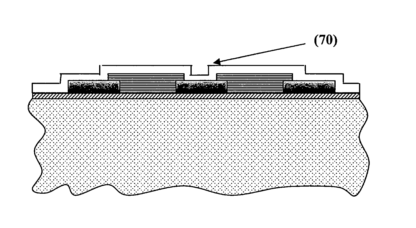
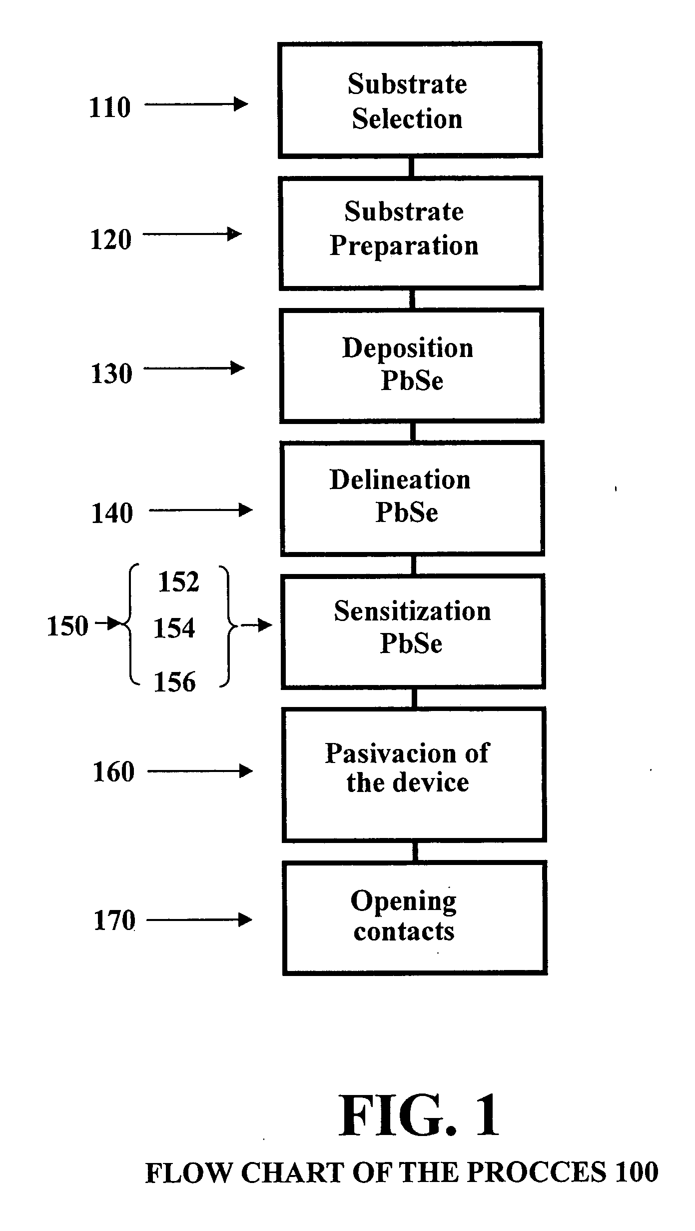
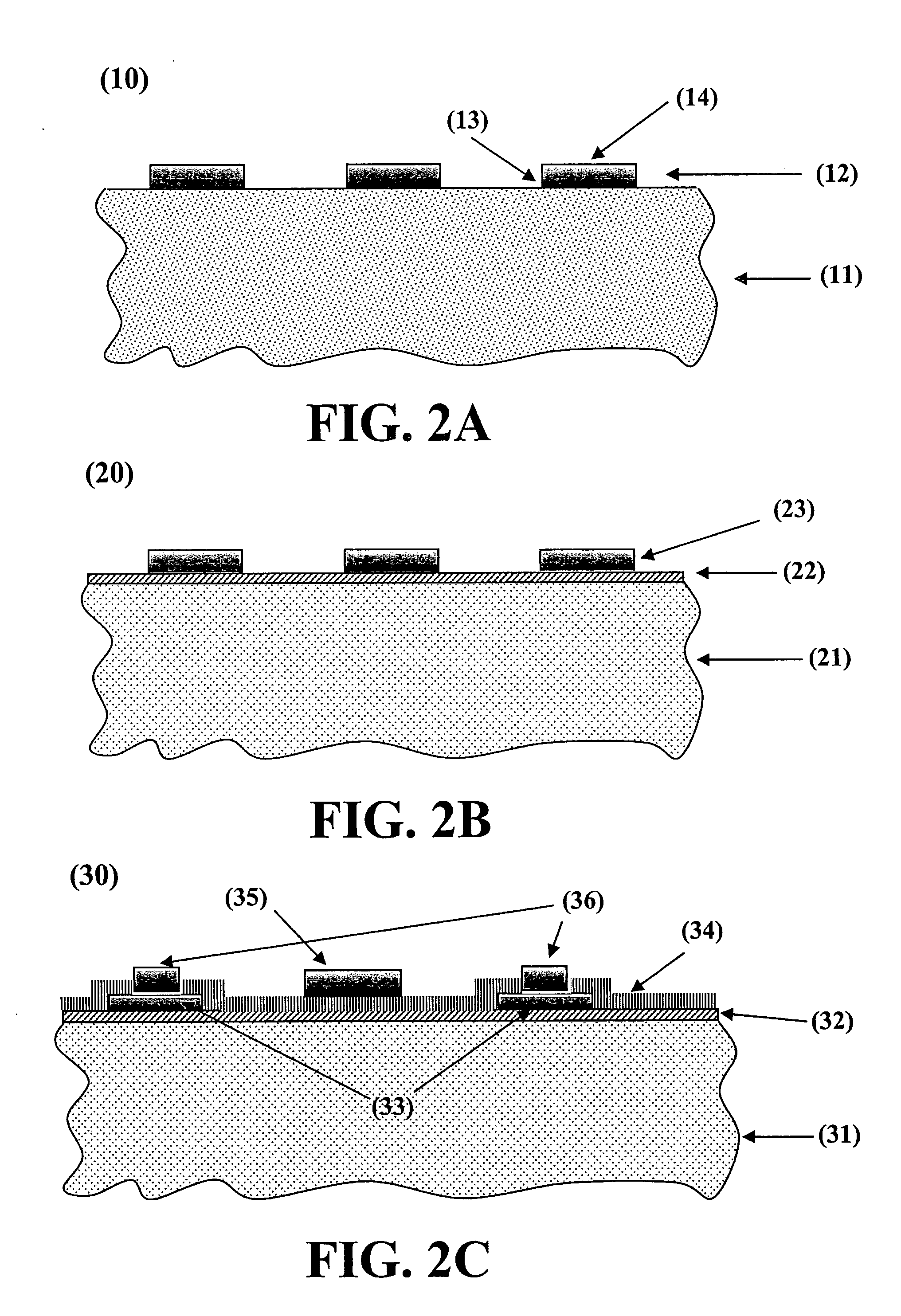
[0017]FIG. 1 shows a flowchart 100 illustrating one embodiment of the method to process polycrystalline lead selenide detectors. The method begins at step 110 by providing a suitable substrate, depending of the type of device to be processed. The method continues at step 120 depositing, insolating and developing a photolithographic resin, leaving free of resin those places selected for depositing PbSe. The method continues at step 130 depositing a layer of PbSe 1-1.2 μm thick by thermal evaporation in vacuum. The method continues at step 140 removing resin and PbSe (lift off), leaving the substrate with well defined detectors onto its surface. The method continues at step 150 submitting the piece (i-substrate) to a sensitizing treatment. It consists in a three folded thermal treatment: at step 152 the piece (i-substrate) is heating up to 290° C. under an atmosphere of oxygen+ iodine during two hour; after, at step 154, the i-substrate is heating up to 430° C. in air during two hours...


PUM

PropertyMeasurementUnit
wavelengthsaaaaaaaaaa
thickaaaaaaaaaa
thickaaaaaaaaaa

Abstract

Method to process polycrystalline lead selenide infrared detectors consisting in: 1) Substrate preparation; 2) Metal deposition; 3) Metal delineation; 4) Sensor delineation; 5) PbSe deposition by thermal evaporation in vacuum; 6) Specific thermal treatment for sensitizing the active material; 7) Deposition of a pasivating layer on the active material. The method is superior to other techniques because permits to process single element detectors, multielement detectors with different geometries such as: linear arrays, 2-dimensional arrays, detectors on interference filters, multicolor arrays and devices monolithically integrated with a ROIC. Applications include low cost infrared detectors for process control, gas analysis, defense, temperature measurement etc.

Description

OBJECT OF THE INVENTION [0001] It is a primary object of the present invention to provide a method to process polycrystalline lead selenide detectors based on thermal evaporation in vacuum followed by an innovative sensitization process consisting on a three folded specific thermal treatment. The method is clearly superior to all previous technologies known to process polycrystalline PbSe two dimensional arrays monolithically integrated with a ROIC, to process x-y addressed two-dimensional arrays and to process multicolor arrays of polycrystalline PbSe detectors. It is still another object of this invention to provide an improved method to process single element polycrystalline lead selenide infrared detectors. It is yet another object of this invention to provide an improved method to process linear arrays of polycrystalline lead selenide infrared detectors. It is still another object of this invention to provide a method to process two-dimensional arrays of polycrystalline lead se...

Claims


Application Information

Patent Timeline
Patent Type & Authority Applications(United States)
IPC IPC(8): G01J5/20
CPCH01L27/1443Y02E10/50H01L31/1864H01L31/0324Y02P70/50
Inventor VERGARA OGANDO, GERMANALMAZAN CARNEROS, ROSAGOMEZ ZAZO, LUIS JORGEVERDU HERCE, MARINARODRIGUEZ FERNANDEZ, PURIFICACIONMONTOJO SUPERVIELLE, MARIA
Owner MINIO DE DEFENSA
Why Eureka
Try Eureka