Thermal release adhesive-backed carrier tapes

a carrier tape and adhesive-backed technology, applied in the direction of semiconductor devices, electrical equipment, semiconductor/solid-state device details, etc., can solve the problems of difficult automated factories, difficult to pick and place ic chips, and difficult methods for packaging these components for automated handling, etc., to achieve repeatable positioning of components, high precision, and high precision

Inactive Publication Date: 2008-01-10
GUTENTAG CHARLES
View PDF3 Cites 19 Cited by
  • Summary
  • Abstract
  • Description
  • Claims
  • Application Information

AI Technical Summary

Benefits of technology

[0014]I have discovered a new mechanism for releasing adhered components to adhesive-backed carrier tapes. It is based on the recognition that with proper choice of the adhesive, i.e. a thermal release adhesive, selectively applied heat will modify the adhesive to eliminate or substantially reduce the component-to-tape peel adhesion. This allows components to be picked from the adhesive-backed carrier tape by action of the pick tool alone, i.e. without mechanical assistance. Thermal release adhesives with fast rise times are preferred, allowing for pick and place cycles of less than one second, e.g., less than 0.5 seconds, and potentially less than 100 milliseconds. Preferred means for applying selective heat in the range of 100 to 120 degrees C. are ceramic heaters. Other choices are arc lamps, tungsten halogen lamps, xenon lamps, lasers, and infrared lamps. Such means of heating could be incorporated in conventional motor driven feeders for punched carrier tape.

Problems solved by technology

As the size of small electronic parts shrinks, methods for packing these components for automated handling become more challenging.
Automated factories cannot function efficiently unless the feedstock components are pre-packed in a uniform, industry standard manner.
Precision pick and place for IC chips is obviously the most challenging due to the small size of the IC chips and the typically demanding tolerances for IC chip placement.
The advent of Chip Sized Packaging (CSP) allows for the packaged component to be similar in size and weight to the Die Product that it contains, making them equally difficult to handle as bare die.
However, there are numerous drawbacks to use of conventional embossed pocket tape and punched cavity tape for handling bare die.1) Absent Industry Standards for bare die products, these devices are produced in virtually any combination of cut size dimensions consistent with form factor requirements and maximum yields per wafer.
Because the cavity size must closely approximate the size of the chip placed therein while allowing ease of chip ingress / egress without restriction, chips are free to move laterally in X-Y- and theta and vertically in angular tilt, resulting in potential damage to die during transit and difficulty in locating and picking extremely small die for retrieval by conventional pick tools.2) Conventional punched and embossed carrier tapes are not suitable for use with micro-sized bare die, which are virtually weightless devices.
Triboelectric charges developed during the peel-back removal will cause micro-size chips to cling to the cover tape.
The extremely low mass of microchips allows them to literally “float” like particles of dust, ignoring the Laws of Gravity.3) The multiplicity of bare die sizes creates a logistics problem for maintaining proper inventories of carrier tapes with fixed cavities, sized to the dimensions of each individual die.
This problem is further intensified by the inevitable consequences of die shrink.4) Bare die products are frequently singulated from silicon wafers, which have been “thinned” to dimensions as small as 25 microns.
Such movement prevents retrieval of individual die from cavities and result in multiple die damage.

Method used


Image

  • Thermal release adhesive-backed carrier tapes
  • Thermal release adhesive-backed carrier tapes
  • Thermal release adhesive-backed carrier tapes

Examples


Embodiment Construction

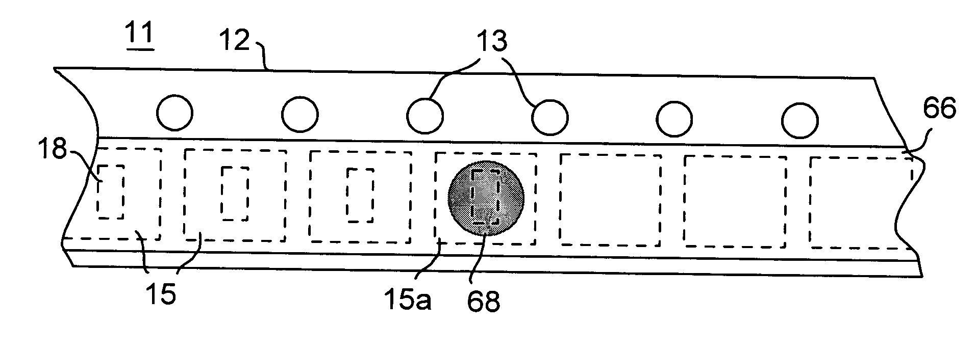
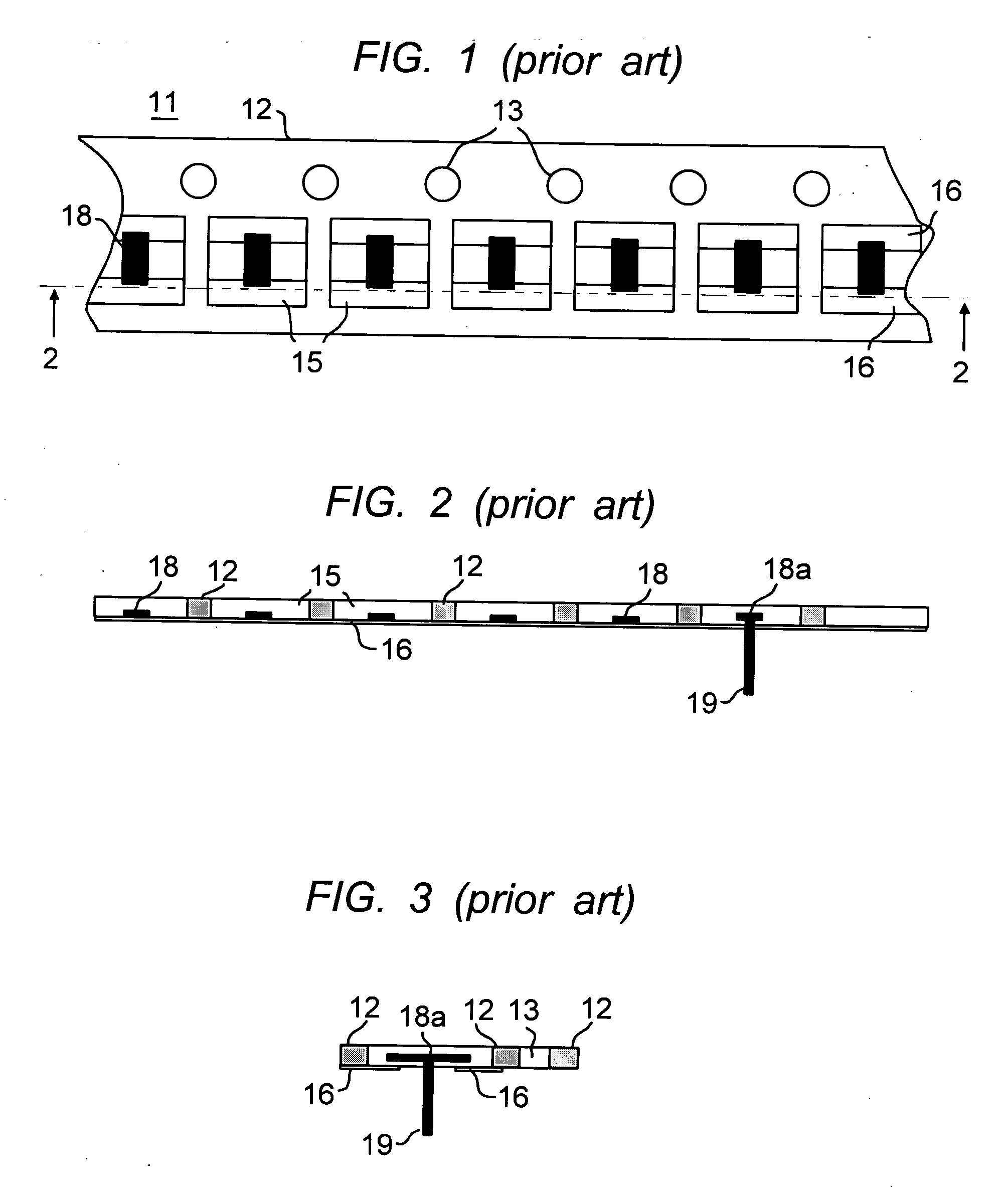
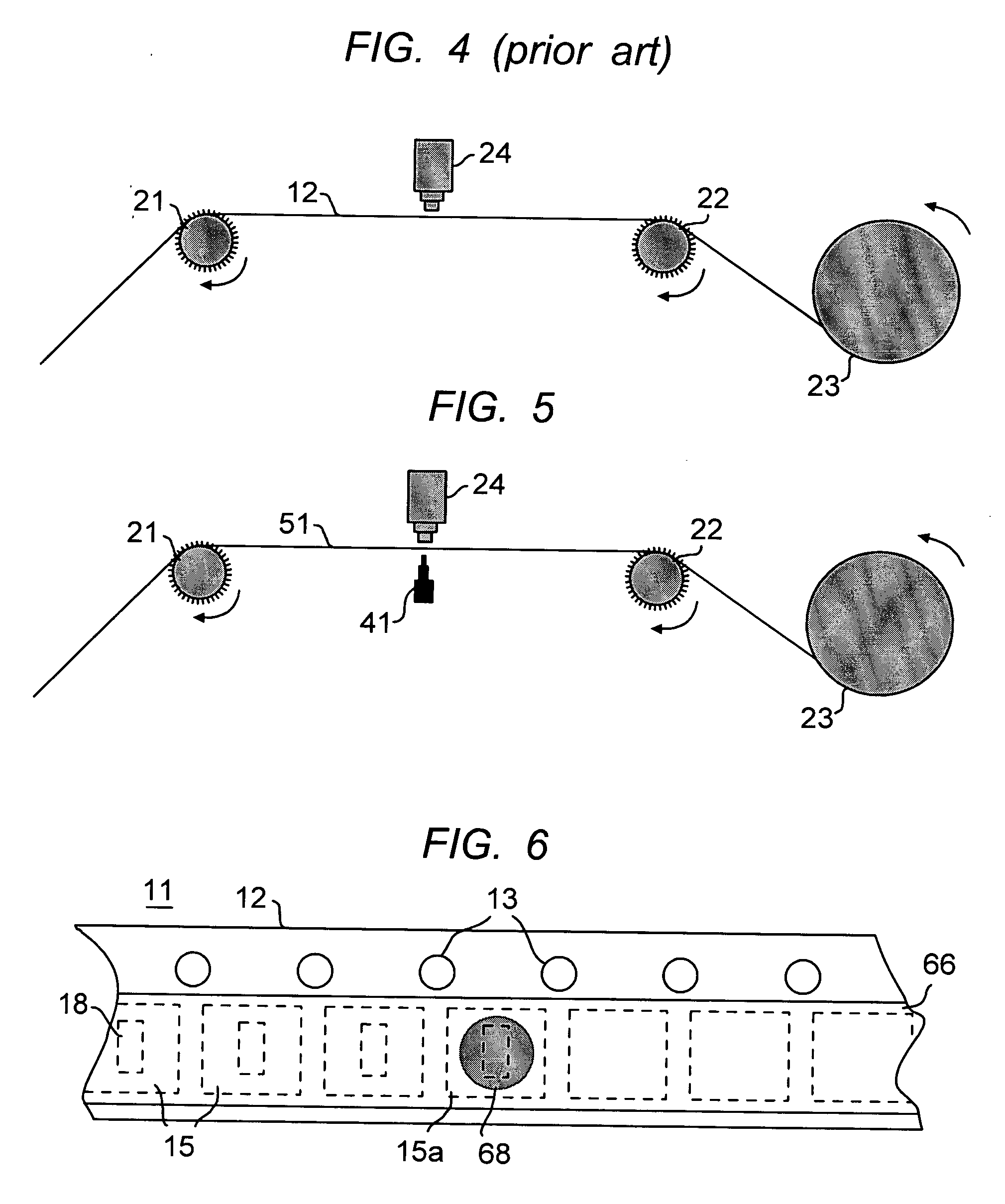
[0024]With reference to FIG. 1, an adhesive-backed carrier tape is shown generally at 11, comprising a continuous length of flexible punched plastic carrier tape 12, sprocket holes 13 for driving and positioning the tape, carrier tape compartments 15, and the pressure-sensitive adhesive backing tape 16. In this illustration the carrier tape compartments are shown loaded with IC chips 18. As indicated above, IC chips 18 are illustrative only of the kinds of parts and components that can be processed using the carrier tape conveyor system of the invention. The pressure sensitive adhesive tape 16 itself is a relatively thin (e.g. 75 micron) continuous tape that is adhesively affixed to the punched plastic carrier tape frame 12.

[0025]The adhesive-backed carrier tape is shown in cross section in FIG. 2. The carrier tape 12 has a front side (top) and a back side (bottom), with chip site openings extending through the chip carrier tape. The chip site openings have an adhesive backing 16 ex...


PUM


Abstract

The specification describes methods for releasing adhered components to adhesive-backed carrier tapes. It is based on the recognition that with proper choice of the adhesive, i.e. a thermal release adhesive, selectively applied heat will modify the adhesive, eliminating or substantially reducing the adhesion between the tape and the IC chip. This allows components to be picked from the adhesive-backed carrier tape without mechanical assistance. Thermal release adhesives having fast rise times are preferred, allowing for pick and place cycles of less than one second, e.g., less than 0.5 seconds. Preferred means for applying selective heat to the adhesive on the carrier tape are ceramic heaters. Other choices are arc lamps, tungsten halogen lamps, xenon lamps, lasers, and infra-red lamps.

Description

FIELD OF THE INVENTION[0001]The field of the invention is storage and transport carrier tape systems for small electronic components. More specifically, it is directed to methods and apparatus for handling small electronic components using thermal release adhesive-backed carrier tapes.BACKGROUND OF THE INVENTION[0002]As the size of small electronic parts shrinks, methods for packing these components for automated handling become more challenging. Automated factories cannot function efficiently unless the feedstock components are pre-packed in a uniform, industry standard manner. In integrated circuit (IC) device manufacture, the individual IC chip size may be less than one millimeter per side. The operative phrase “Die Shrink” is a principle objective of silicon wafer fabricators for two primary reasons: (1) the continuing demand for smaller, lighter, consumer electronic devices with additional performance features (led by mobile telephones) which require more functions within small...

Claims


Application Information

Patent Timeline
Patent Type & Authority Applications(United States)
IPC IPC(8): H01L23/02
CPCH01L21/67132H01L21/6835H01L2924/1461H01L24/86H01L2221/68322H01L2221/68354H01L2224/7965H01L2924/01027H01L2924/01042H01L2924/01054H01L2924/01074H01L2924/14H01L2924/19041H01L2924/19042H01L2924/19043H01L2924/01005H01L2924/01006H01L2924/01033H01L2924/00
Inventor GUTENTAG, CHARLES
Owner GUTENTAG CHARLES
Why Eureka
Try Eureka