Via hole forming method

a technology of via hole and forming method, which is applied in the direction of printed circuit manufacturing, semiconductor/solid-state device details, manufacturing tools, etc., can solve the problems of reducing the quality of each device, reducing the productivity of each device, and not always satisfying the productivity of drilling via holes, so as to achieve efficient drilling and form the effect of efficient drilling

Inactive Publication Date: 2008-01-10
DISCO CORP
View PDF5 Cites 11 Cited by
  • Summary
  • Abstract
  • Description
  • Claims
  • Application Information

AI Technical Summary

Benefits of technology

[0016]In the via hole forming method of the present invention, as the pulse laser beam applied in the first step has an energy density (40 to 60 J/cm2 per pulse) capable of processing a semiconductor substrate made of silicon efficiently, holes can be formed efficiently. The unprocessed portions formed in the first step are processed by applying a pulse laser beam havin

Problems solved by technology

Therefore, the diameters of the via holes formed in the semiconductor wafer are as small as 100 to 300 μm, and drilling the via holes is not always satisfactory in terms of productivity.
Although a conductive material such as aluminum or copper is buried in the via holes formed in the substrate as described above, when aluminum or coppe

Method used


Image

  • Via hole forming method
  • Via hole forming method
  • Via hole forming method

Examples


Embodiment Construction

[0025]A preferred embodiment of the present invention will be described in detail hereinbelow with reference to the accompanying drawings.

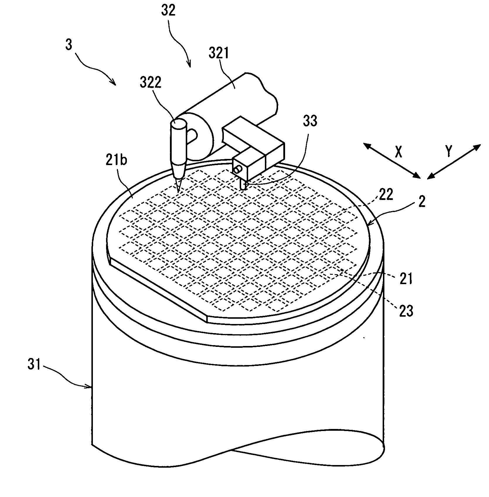
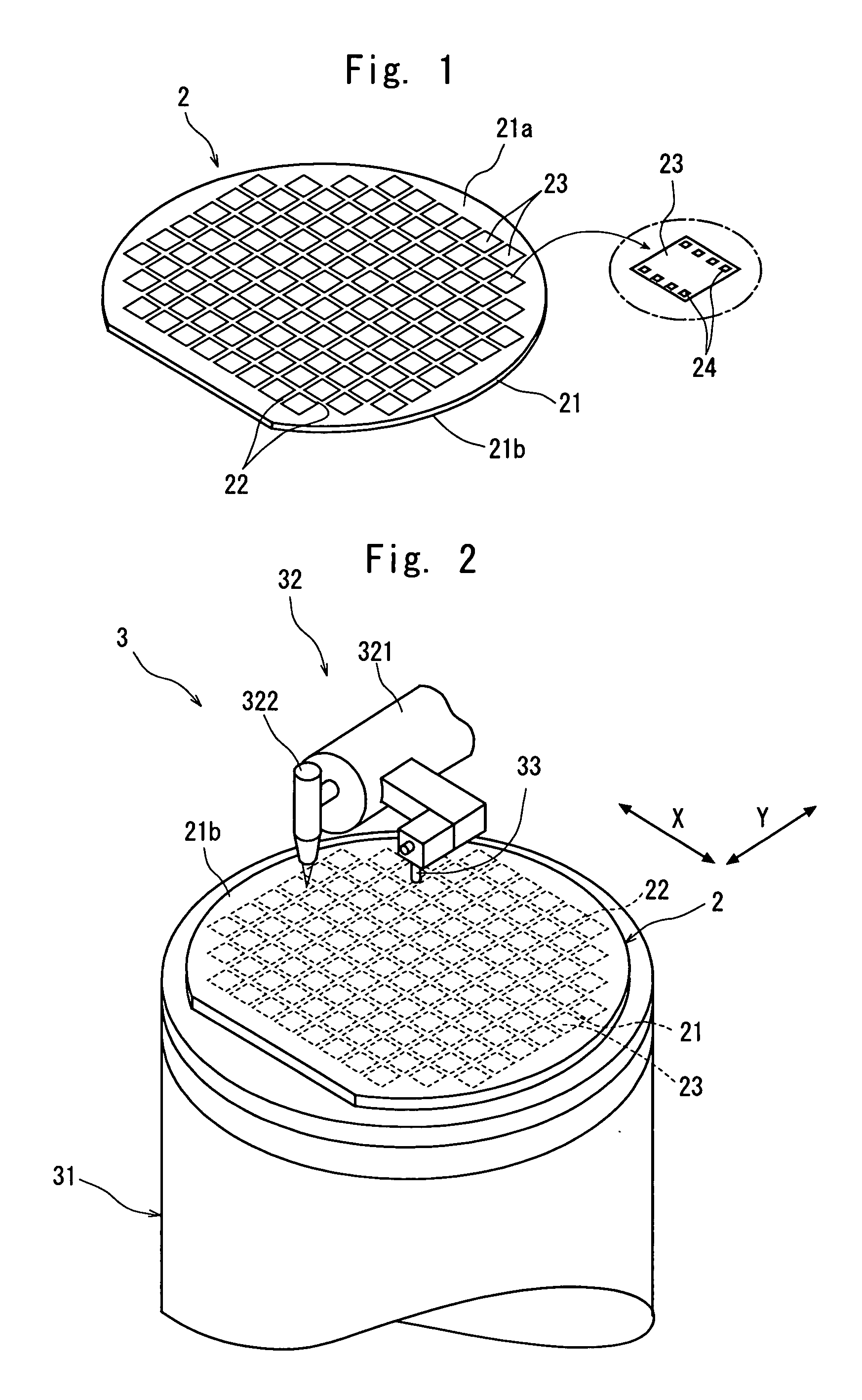
[0026]FIG. 1 is a perspective view of a semiconductor wafer 2 as the wafer to be processed by the via hole forming method of the present invention. In the semiconductor wafer 2 shown in FIG. 1, a plurality of areas are defined by a plurality of streets 22 arranged in a lattice on the front surface 21a of a substrate 21 made of silicon and having a thickness of, for example, 100 μm, and a device 23 such as IC or LSI is formed in each of the defined areas. The devices 23 are the same in structure. A plurality of bonding pads 24 are formed on the surface of each device 23. The bonding pads 24 are made of a metal material such as aluminum, copper, gold, platinum or nickel and have a thickness of 1 to 5 μm.

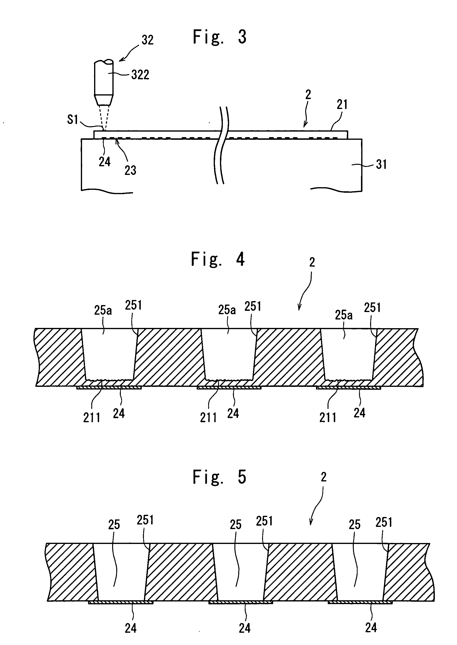
[0027]Via holes reaching the bonding pads 24 are formed in the above semiconductor wafer 2 by applying a pulse laser beam to the rear surface 21b of...


PUM

PropertyMeasurementUnit
Electric dipole momentaaaaaaaaaa
Diameteraaaaaaaaaa

Abstract

A method of forming a via hole reaching a bonding pad in a wafer having a plurality of devices formed on the front surface of a substrate and bonding pads formed on each of the devices by applying a pulse laser beam to the rear surface of the substrate, the method comprising the steps of:
    • forming a non-through hole having a predetermined depth in the front surface of the substrate by applying a pulse laser beam having a spot diameter of 0.75 to 0.9 D when the diameter of the via hole to be formed is represented by D and an energy density per pulse of 40 to 60 J/cm2 to the rear surface of the substrate; and
    • forming a via hole reaching a bonding pad in the substrate by applying a pulse laser beam having an energy density per pulse of 25 to 35 J/cm2 to the hole formed in the substrate.

Description

[0001]1. Field of the Invention[0002]The present invention relates to a method of forming a via hole reaching a bonding pad in a wafer having a plurality of devices on the front surface of a substrate and bonding pads on each of the devices by applying a pulse laser beam to the rear surface of the substrate.[0003]2. Description of the Prior Art[0004]In the production process of a semiconductor device, a plurality of areas are defined by dividing lines called “streets” arranged in a lattice on the front surface of a substantially disk-like semiconductor wafer, and a device such as IC or LSI is formed in each of the defined areas. Individual semiconductor chips are manufactured by cutting this semiconductor wafer along the streets to divide it into the device formed areas.[0005]To reduce the size and to increase the number of functions of an apparatus, a modular structure for connecting the bonding pads of a plurality of semiconductor chips which are formed in a layer has been impleme...

Claims


Application Information

Patent Timeline
IPC IPC(8): H01L21/4763B23K26/00B23K26/16B23K26/382H01L21/768H01L23/522H01L25/07H01L25/18H05K3/00
CPCH01L21/76898H01L2924/0002H01L2924/00
Inventor MORIKAZU, HIROSHI
Owner DISCO CORP
Why Eureka
Try Eureka