Microphotonic maskless lithography

a maskless lithography and microphotonic technology, applied in the field of microfabrication and nanofabrication, can solve the problems of high exposure speed of maskless lithography system, and achieve the effects of high modulation speed, easy scaling, and high number of parallel photon beams

Active Publication Date: 2008-01-17
MASSACHUSETTS INST OF TECH
View PDF92 Cites 43 Cited by
  • Summary
  • Abstract
  • Description
  • Claims
  • Application Information

AI Technical Summary

Benefits of technology

[0007] Embodiments of the invention feature a completely integrated solution fully compatible with planar processing. Hence, embodiments of the invention are easily scalable. This allows for a high number of parallel photon beams. Moreover, the use of in-plane modulators allows for higher modulation speed than out-of-plane modulators. This results in high exposure speeds for a maskless lithography system. A conservative estimate of an exemplary exposure speed of the disclosed technology may be attained by assuming a modulation speed of 1 GHz (40 GHz in-plane modulators have already been demonstrated) and 1000 photon beams (easily achievable with today's technology). The resulting exposure speed is around one terapixel per second.

Problems solved by technology

This results in high exposure speeds for a maskless lithography system.

Method used


Image

  • Microphotonic maskless lithography
  • Microphotonic maskless lithography
  • Microphotonic maskless lithography

Examples


Embodiment Construction

Definitions

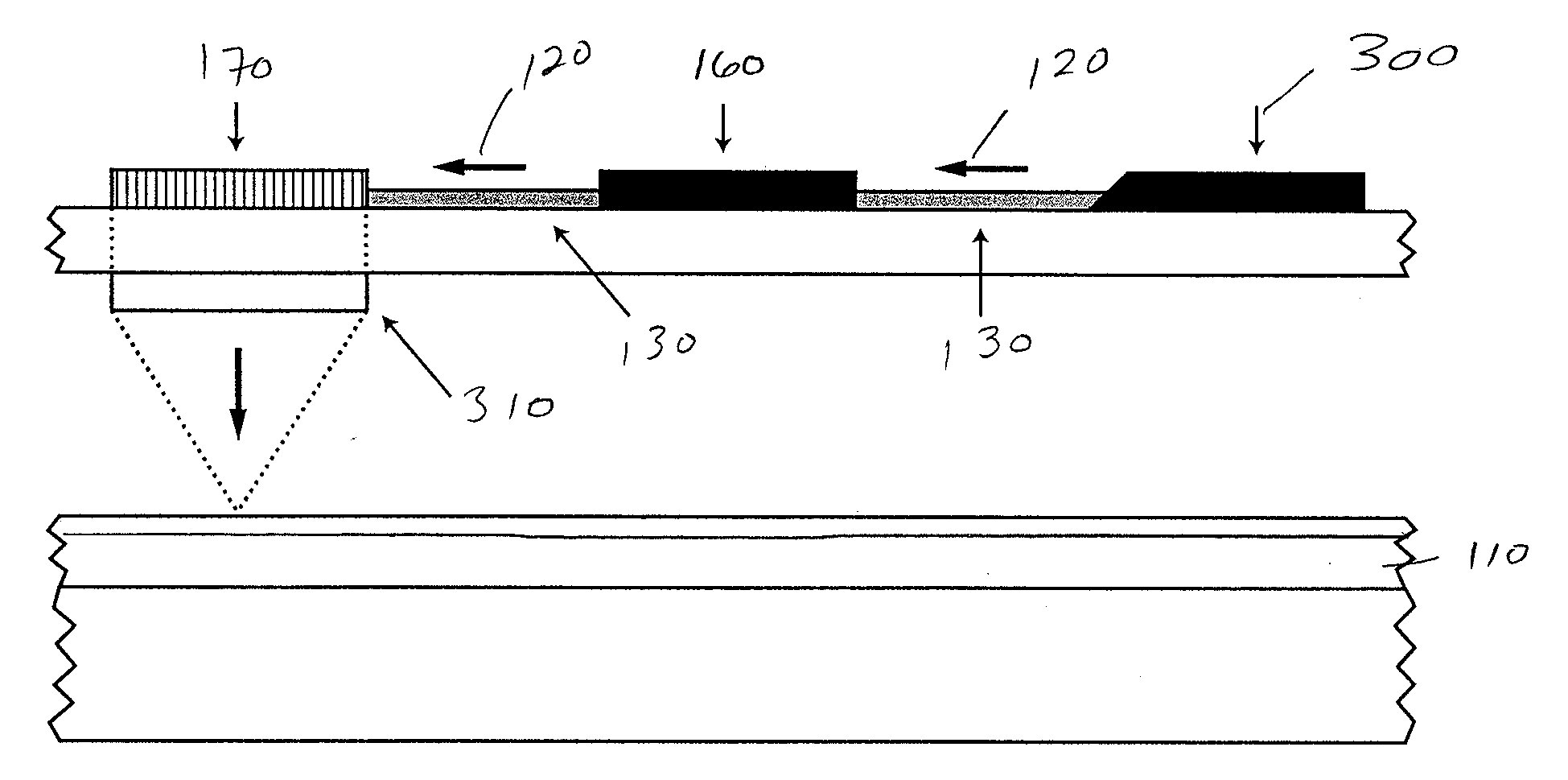
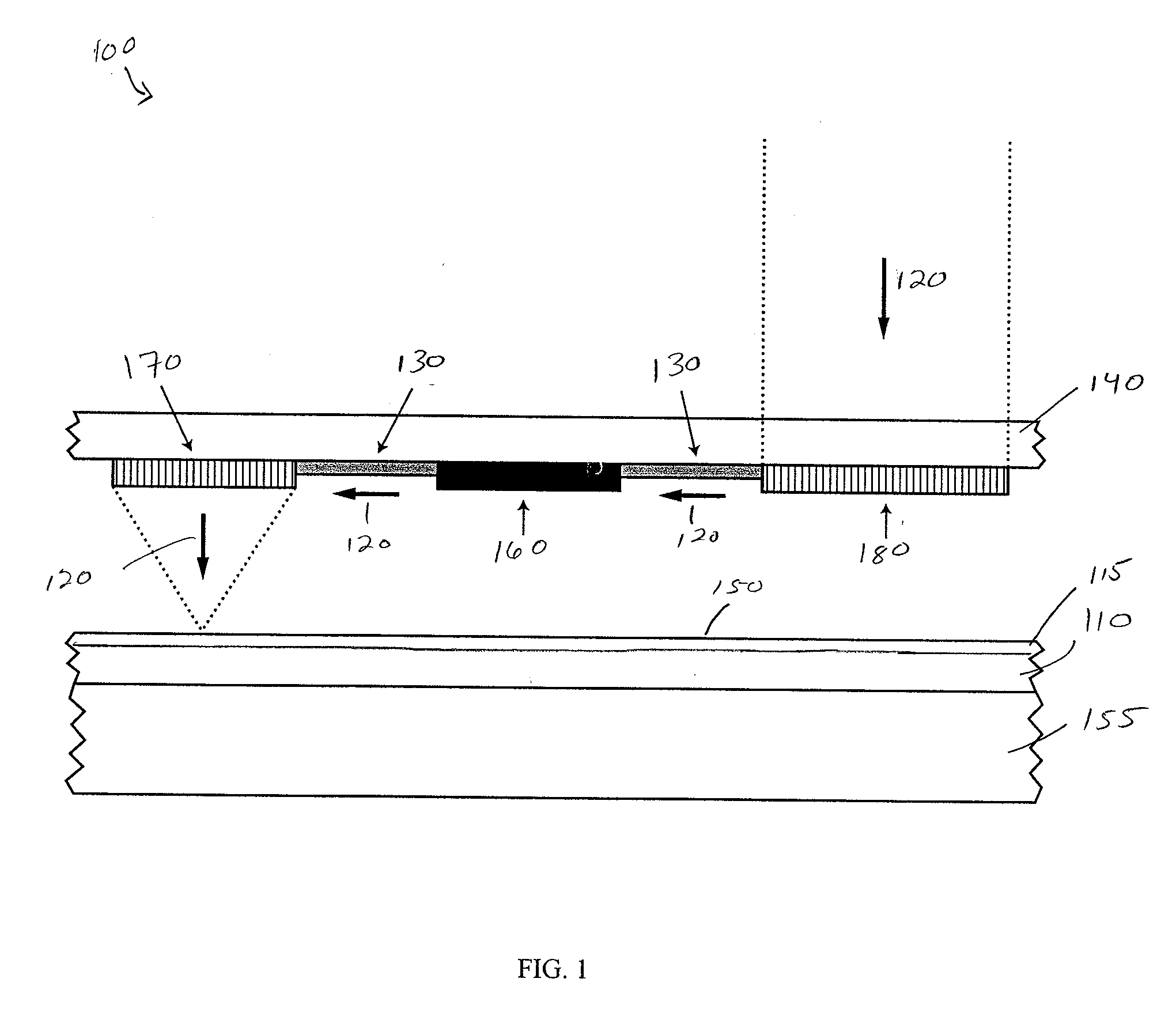
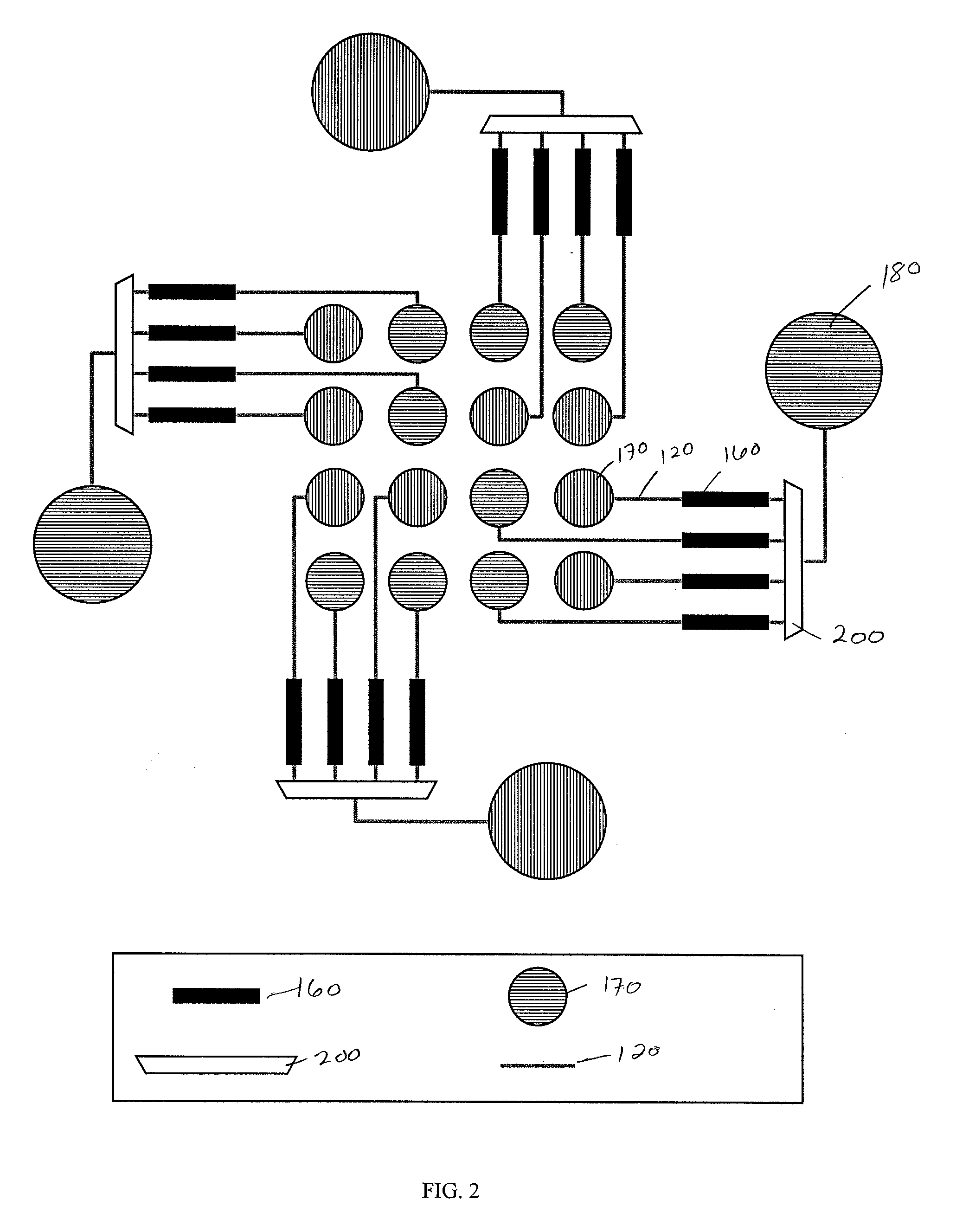
[0025] As used herein, the term waveguide means a structure that can guide a photon beam. This includes but is not limited to dielectric waveguides such as rib waveguides, ridge waveguides, strip waveguides, wire waveguides, and rectangular waveguides. Any waveguide design may be employed in embodiments of the present invention.

[0026] As used herein, the term vertical coupler means a structure that can couple a photon beam from free space to a waveguide while changing the direction of the photon beam significantly. Hence, the directions of propagation of the beam in free space and in the waveguide differ by a significant angle. A vertical coupler also works in the reverse direction. It couples a photon beam from a waveguide to free-space while changing the direction of the photon beam significantly. A free-space photon beam emerging from a vertical coupler can be focused or not focused by the vertical coupler, depending on the design of the vertical coupler. Vertical co...


PUM

PropertyMeasurementUnit
wavelengthaaaaaaaaaa
distanceaaaaaaaaaa

Abstract

A maskless lithography system and method to expose a pattern on a wafer by propagating a photon beam through a waveguide on a substrate in a plane parallel to a top surface of the wafer.

Description

RELATED APPLICATIONS [0001] This application claims the benefit of and priority to U.S. Provisional Application Ser. No. 60 / 830,126 filed Jul. 11, 2006, the entire disclosure of which is hereby incorporated by reference.FIELD OF THE INVENTION [0002] The technology disclosed herein relates generally to microfabrication and nanofabrication and, more specifically, to lithography. BACKGROUND [0003] In general, lithography is a necessary step in planar processing of microstructures and nanostructures. It is the step defining the in-plane shape of the structures. One may distinguish between lithographic systems employing a mask and systems not employing masks. The latter are referred to as maskless lithography systems. Lithographic systems employing a mask have the advantage of being able to replicate the mask pattern on substrates at high speed. This is the case in projection lithography, contact lithography, imprint lithography, EUV lithography, and x-ray lithography, which are typicall...

Claims


Application Information

Patent Timeline
Patent Type & Authority Applications(United States)
IPC IPC(8): G03B27/54G03F7/20
CPCG03F7/70383
Inventor BARWICZ, TYMONPOPOVIC, MILOS
Owner MASSACHUSETTS INST OF TECH
Why Eureka
Try Eureka