Method for fabricating color filters

Inactive Publication Date: 2008-01-24
UNITED MICROELECTRONICS CORP +1
View PDF3 Cites 27 Cited by
  • Summary
  • Abstract
  • Description
  • Claims
  • Application Information

AI Technical Summary

Benefits of technology

[0013]By performing a pattern transfer process to form a trench in the dielectric layer disposed on the substrate, depositing a color filter in the trench, and performing a chemical mechanical polishing process to planarize the surface of the color filter, the present invention is able to improve the problem of poor resolution

Problems solved by technology

Due to the temperature limitation, the color filter array fabricated by the lift-off process is unable to provide color filters with optimal optical property.
However, by performing a series of pattern transfer and etching process on the color filter material directly, the etchant used by the aforemen

Method used


Image

  • Method for fabricating color filters
  • Method for fabricating color filters
  • Method for fabricating color filters

Examples


Embodiment Construction

[0019]Certain terms are used throughout the following description and claims to refer to particular system components. As one skilled in the art will appreciate, consumer electronic equipment manufacturers may refer to a component by different names. This document does not intend to distinguish between components that differ in name but not function. In the following discussion and in the claims, the terms “including” and “comprising” are used in an open-ended fashion, and thus should be interpreted to mean “including, but not limited to . . . ” The terms “couple” and “couples” are intended to mean either an indirect or a direct electrical connection. Thus, if a first device couples to a second device, that connection may be through a direct electrical connection, or through an indirect electrical connection via other devices and connections.

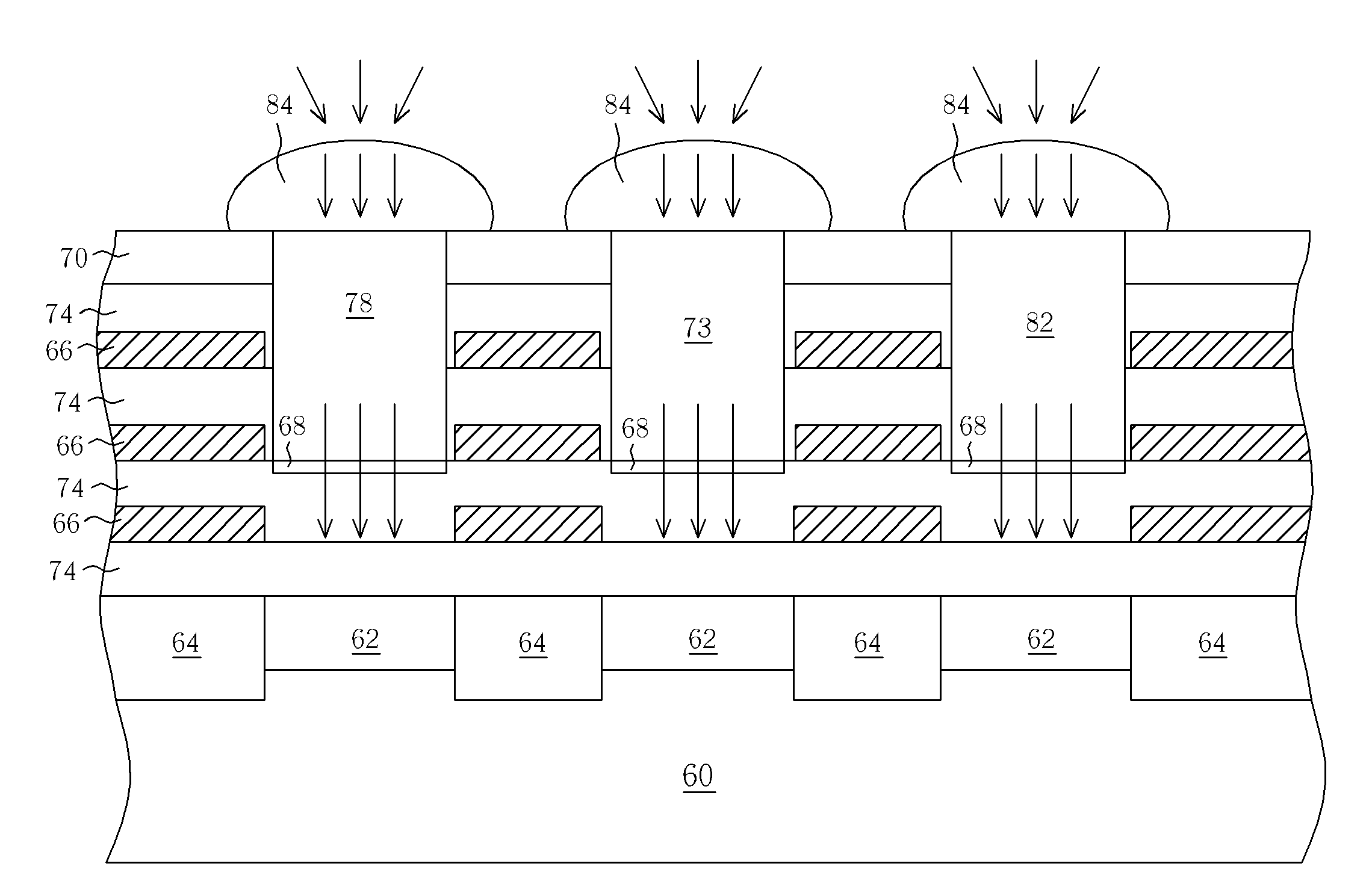
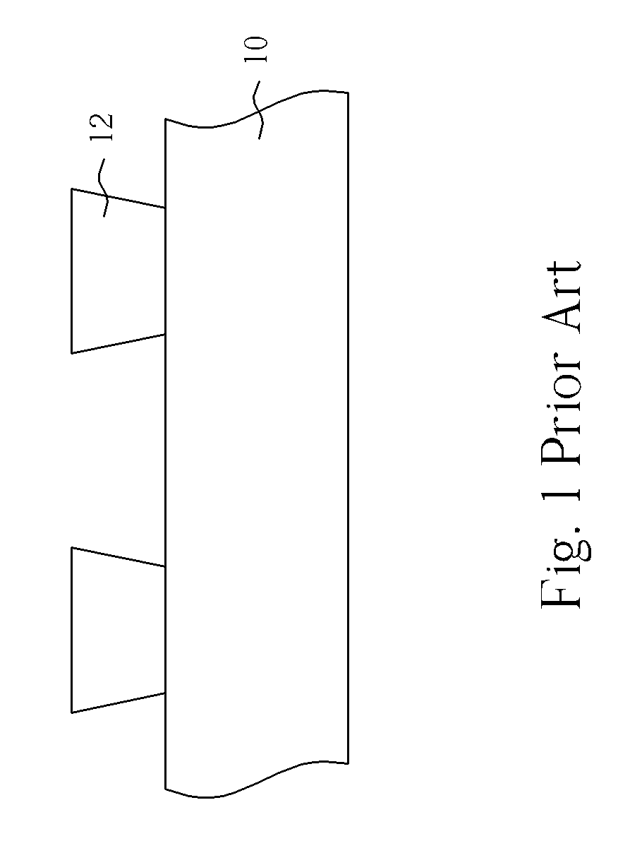
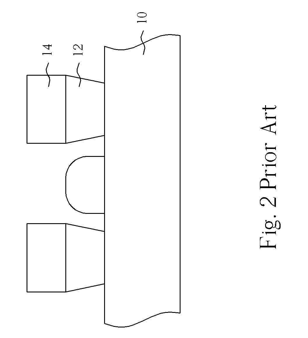
[0020]Please refer to FIG. 10 through FIG. 14. FIG. 10 through FIG. 14 are perspective diagrams showing a method of fabricating a color filter ...


PUM


Abstract

A method for fabricating a color filter is disclosed. First, a substrate having a dielectric layer and a passivation thereon is provided. Next, a first pattern transfer process is performed to form a trench in the dielectric layer and the passivation layer, and a color filter is formed in the trench, in which the color filter partially covers the surface of the passivation layer. Next, a chemical mechanical polishing process is performed to planarize the color filter, such that the surface of the color filter is even with the surface of the passivation layer.

Description

BACKGROUND OF THE INVENTION[0001]1. Field of the Invention[0002]The invention relates to a method for fabricating color filters.[0003]2. Description of the Prior Art[0004]As the development of electronic products progresses, the demand for related components has increased as well. For example, as the development of digital cameras and scanners progresses, the demand for image sensor increases accordingly. In general, today's image sensors in common usage are divided into two main categories: charge coupled device (CCD) sensors and CMO image sensors (CIS). The application of CMOS image sensors has increased significantly for several reasons. Primarily, CMOS image sensors have certain advantages of offering low operating voltage, low power consumption, and the ability for random access. Additionally, CMOS image sensors are currently capable of integration with the semiconductor fabrication process.[0005]The CMOS image sensor separates (i.e., classifies) incident light into a combinati...

Claims


Application Information

Patent Timeline
IPC IPC(8): H01L31/00G02B5/20
CPCG02B5/201H01L27/14685H01L27/14627H01L27/14621
Inventor WU, YI-TYNGOU, FU-KUOKUAN, TA-SHUANG
Owner UNITED MICROELECTRONICS CORP
Why Eureka
Try Eureka