
Spatial light modulator features

a spatial light modulator and features technology, applied in the field of heat-minimizing spatial light modulators, can solve the problems of extremely long development time for prototyping any kind of electronic circuit, increased mask cost for integrated circuit fabrication, and inability to meet the needs of the user, so as to achieve the effect of eliminating the source and higher resolution

Active Publication Date: 2008-01-24
NAT TECH & ENG SOLUTIONS OF SANDIA LLC
View PDF2 Cites 6 Cited by
  • Summary
  • Abstract
  • Description
  • Claims
  • Application Information

AI Technical Summary

Benefits of technology

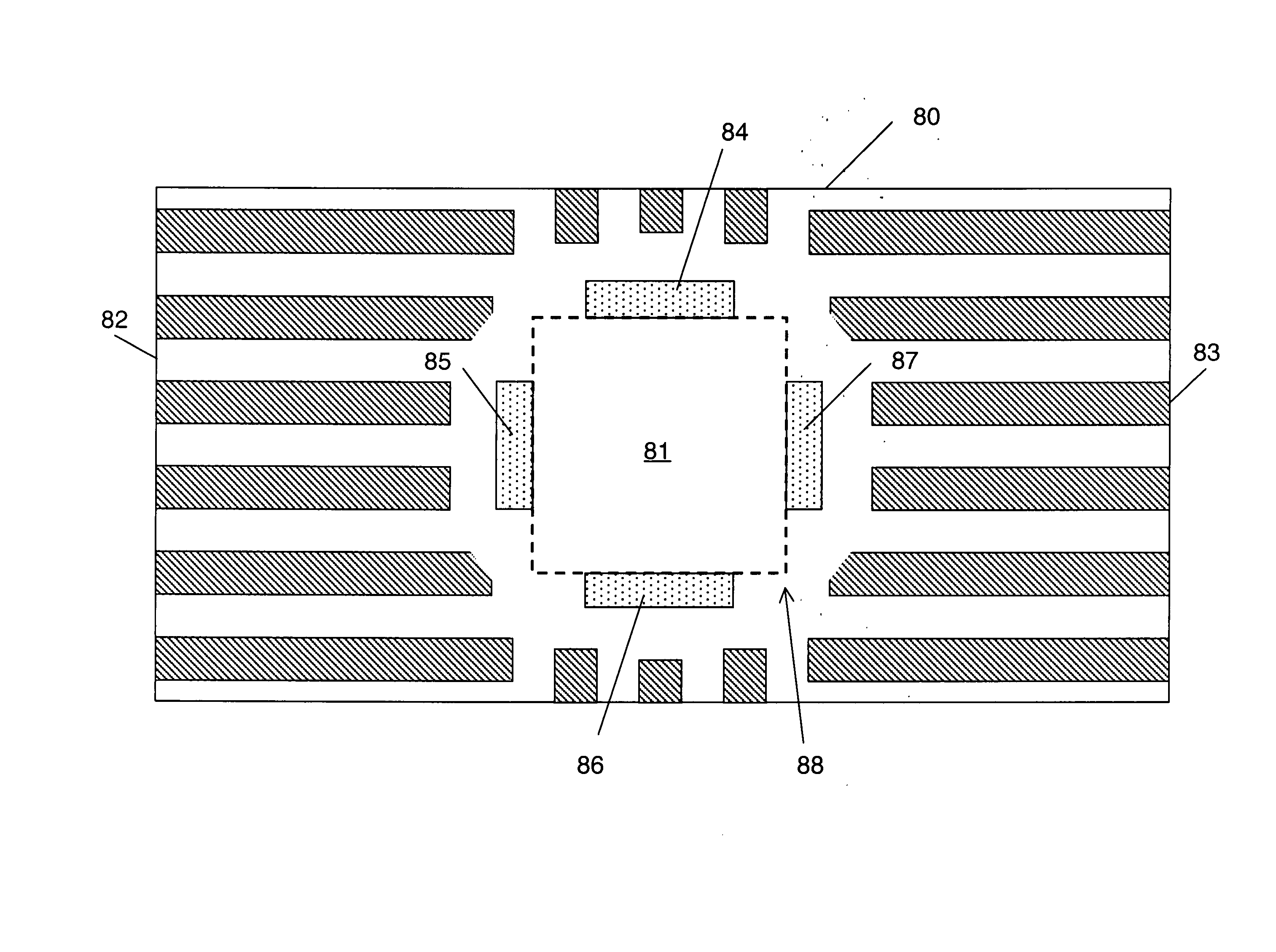
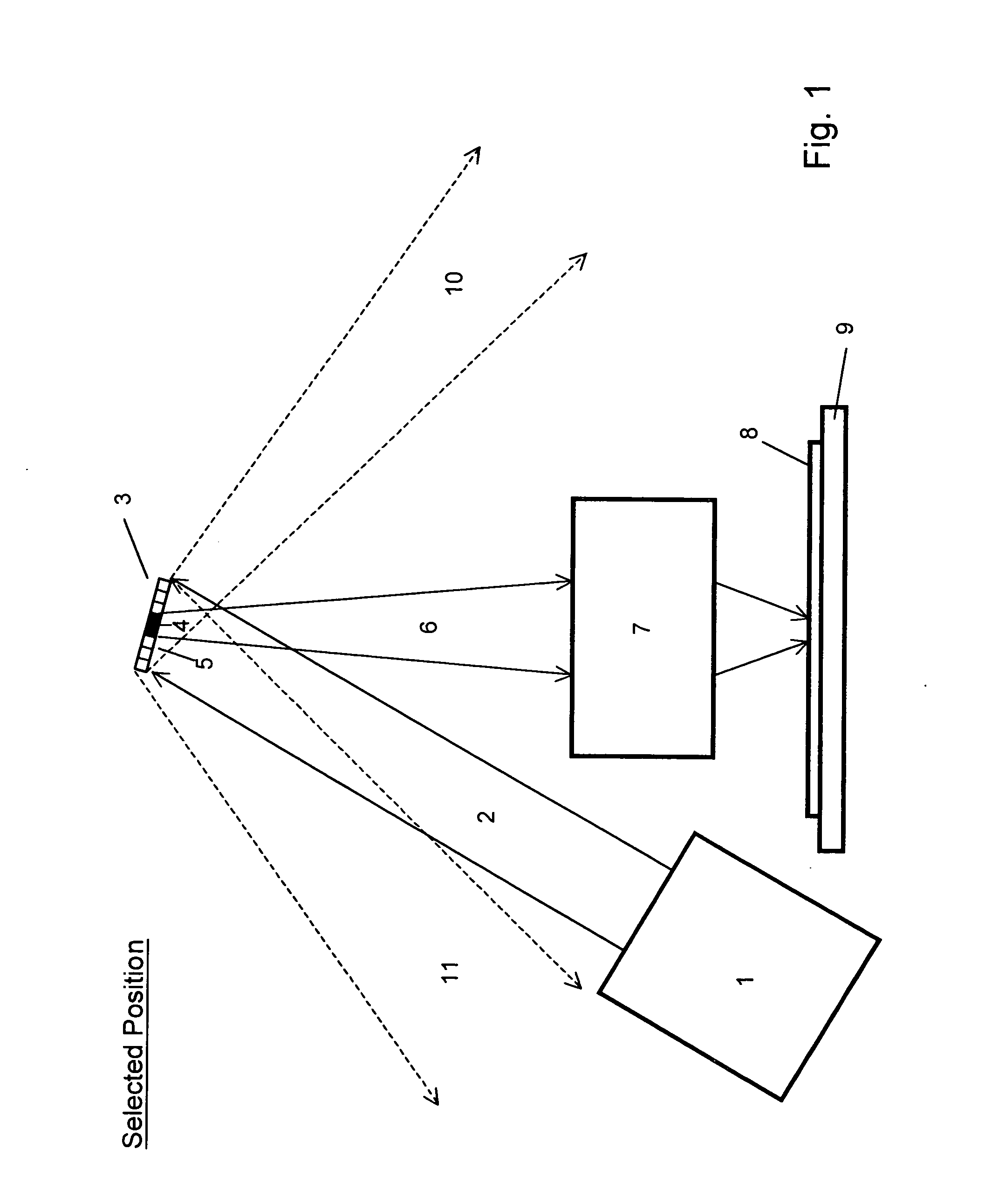
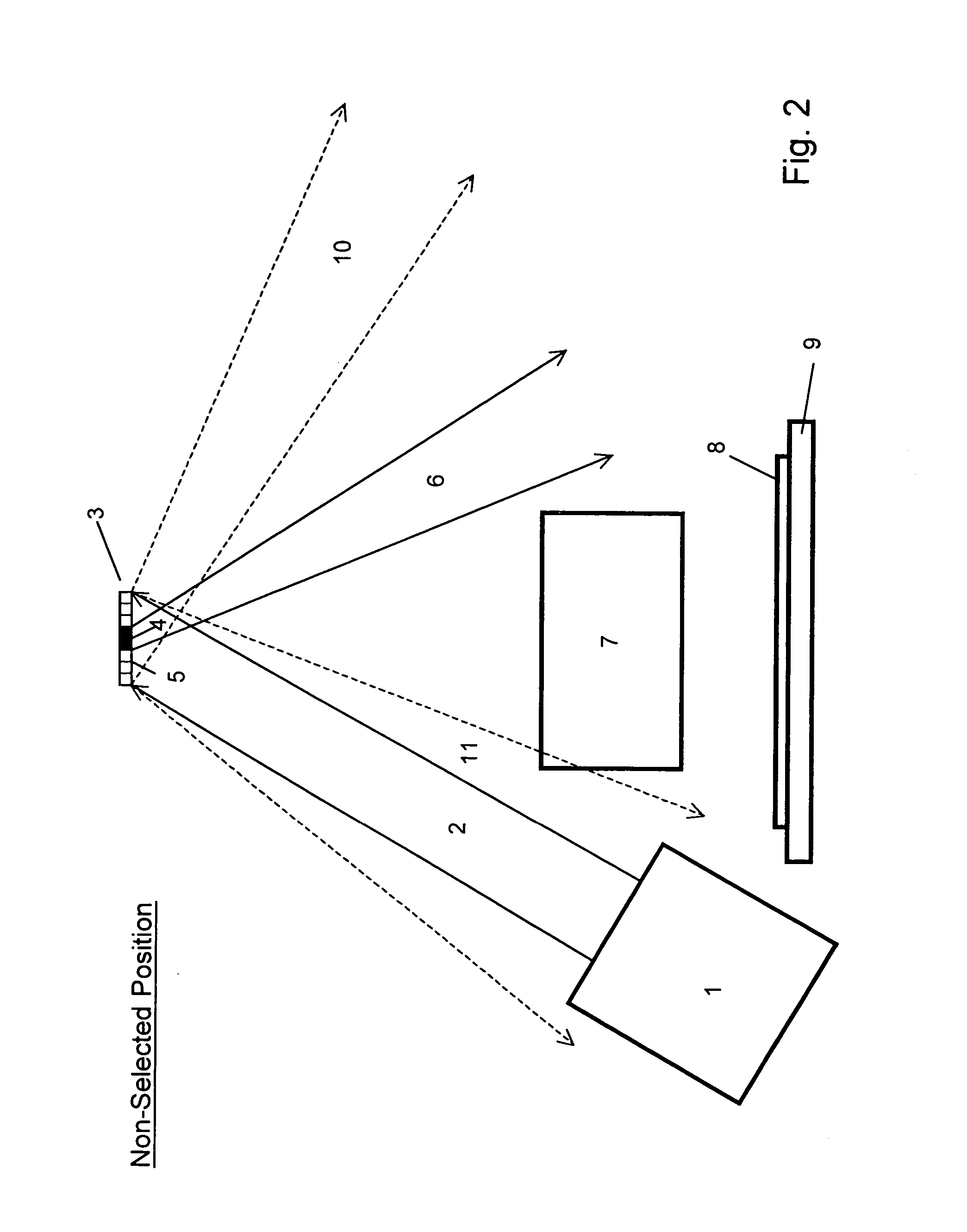
This patent describes a technology that helps to prevent heat build-up in a type of light modulator used in projection systems. This technology uses special devices called diffracting digital micromirror devices (DDMD) that have additional features to enhance the resolution of the projected image. These features include reflective phase grating and mirror elements that redirect the illumination radiation incident on the non-mirror portion of the pixel surface, eliminating a source of deleterious heating. The redirected beam or beams are then directed through the projection lens to form an image with higher resolution than could be achieved with simple mirror pixels. Overall, this technology allows for very-large-scale systems of spatial light modulators and targets to operate without destructive heating effects.

Problems solved by technology

As the minimum feature sizes of semiconductor devices continue to shrink, the cost of masks for integrated circuit fabrication continues to increase, now exceeding a million dollars for a mask set for the leading devices.
This leads to extremely long development times for prototyping any kind of electronic circuit.
Since it is not possible in such a production scenario to amortize the high mask costs over large volumes, the mask costs become especially unbearable.
This can result in a different problem, however, since the self-protective nature of the typical fully-mirrorized pixel element is diminished greatly—namely, heating of the spatial light modulator array by the non-reflected majority (⅞ths) of the incident radiation.
These desired frequencies, however, when present at power levels typical to patterning systems and projection display systems, are significant sources of heat when absorbed by the majority non-reflective areas of a spatial light modulator in which the reflective area is only a small portion of the total pixel element area.
The repetitive nature of the typical patterning system, and the constant nature of the typical display system, can cause such systems to suffer damage by destructive heat buildup, e.g., degradation of the DMD, its driver electronics, optical components, and their coatings.

Method used


Image

  • Spatial light modulator features
  • Spatial light modulator features
  • Spatial light modulator features

Examples


Embodiment Construction

[0029] General Considerations

[0030] Spatial light modulator (SLM) arrays are used in maskless lithography and other applications. A variety of SLMs have been employed for use with different wavelengths. The most widely investigated type of SLM comprises a 2-D array of micromirrors fabricated in Si wafers with process technologies similar to those used in IC production. In these SLMs, typically the size of an individual micromirror element (pixel) is approximately 15×15 μm. When used in lithography, the achievable system resolution and throughput depend on the pixel size and number of pixels. It is highly desirable to make the size of each pixel as small as possible and the number of pixels in an SLM array as large as possible. For example, with advanced microelectromechanical systems (MEMS) technologies, it is possible to make an SLM array with a grid size of 4×8 μm, with a total number of micromirrors as large as 108-109.

[0031] By minimizing the size of the pixels, it is possible...


PUM

PropertyMeasurementUnit
sizeaaaaaaaaaa
sizeaaaaaaaaaa
sizeaaaaaaaaaa

Abstract

An enhanced spatial light modulator (ESLM) array, a microelectronics patterning system and a projection display system using such an ESLM for heat-minimization and resolution enhancement during imaging, and the method for fabricating such an ESLM array. The ESLM array includes, in each individual pixel element, a small pixel mirror (reflective region) and a much larger pixel surround. Each pixel surround includes diffraction-grating regions and resolution-enhancement regions. During imaging, a selected pixel mirror reflects a selected-pixel beamlet into the capture angle of a projection lens, while the diffraction grating of the pixel surround redirects heat-producing unused radiation away from the projection lens. The resolution-enhancement regions of selected pixels provide phase shifts that increase effective modulation-transfer function in imaging. All of the non-selected pixel surrounds redirect all radiation energy away from the projection lens. All elements of the ESLM are fabricated by deposition, patterning, etching and other microelectronic process technologies.

Description

CROSS-REFERENCE TO RELATED APPLICATIONS [0001] This is a divisional application of U.S. patent application Ser. No. 11 / 237,382, filed Sep. 28, 2005, now U.S. Pat. No. ______, Issue date ______, Jain et al., SPATIAL LIGHT MODIULATOR ARRAY WITH HEAT MINIMIZATION AND IMAGE ENHANCEMENT FEATURES.BACKGROUND OF THE INVENTION [0002] (1) Field of the Invention [0003] This invention relates to a heat-minimizing spatial light modulator with image enhancement features based on diffracting digital micromirror devices (DDMDs) and to techniques for fabricating and incorporating DDMDs in projection optical imaging and patterning systems. [0004] (2) Description of the Related Art [0005] A maskless lithography technology that is capable of high-resolution patterning is essential for manufacturing of many microelectronic and bio-molecular devices. Lithographic techniques using conventional masks involve a multi-step process which includes defining the desired features on the mask which is then used to...

Claims


Application Information

Patent Timeline
Patent Type & Authority Applications(United States)
IPC IPC(8): G02B26/02G03B21/28G03B27/70G03C5/56
CPCG03F7/70291G02B26/0808
Inventor JAIN, KANTISWEATT, WILLIAM C.ZEMEL, MARC
Owner NAT TECH & ENG SOLUTIONS OF SANDIA LLC
Learn More