

Light emitting device containing phosphorescent complex
a light emitting device and phosphorescent complex technology, applied in the direction of discharge tube luminescnet screens, other domestic articles, natural mineral layered products, etc., can solve the problems of large loss of efficiency, performance limitations that have been a barrier to many desirable applications, etc., to improve device drive voltage, efficiency, and lifetime.
- Summary
- Abstract
- Description
- Claims
- Application Information
AI Technical Summary
Benefits of technology
Problems solved by technology
Method used
Image

Examples
examples
[0303]Ligand Preparation: o-hydoxycarbonylbenzene (40 mmol) and 2-pyridylacetonitrile (40 mmol) were added to an aqueous solution of NaOH (0.05 N, 200 ml). The mixture was vigorously stirred at 90° C. for 3.5 hours. After cooling the solid was filtered, washed with cold water and dried. The crude compound was purified by crystallization from ethanol yield: 92%. MS: m / z calcd 223; found 224; [M+1].[0304]Synthesis of Ir(3-pyridylcoumarin)2(acac) (Ir(pcm)2acac): Cyclometalated Ir(III) μ-chloro-bridged dimer of (pcm)2Ir(μ-Cl)2Ir(pcm)2 was synthesized according to the Nonoyama route, by refluxing IrCl3.nH2O with 2-2.5 equiv of 3-pyridylcoumarin in a 3:1 mixture of 2-ethoxyethanol and water. The chloro-bridged dimer complex (0.08 mmol), 0.2 mmol of acetyl acetone, and 85-90 mg of sodium carbonate were heated to reflux in dichloroethane under an inert atmosphere for 12-15 hours. After cooling, the mixture was extracted with water, dried with MgSO4, and concentrated. The crude product was p...
examples 1-1 through 1-6
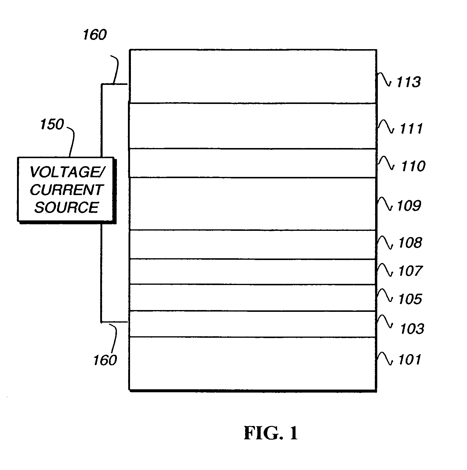
[0310]EL devices (Examples 1-1 through 1-6) satisfying the requirements of the invention were constructed in the following manner:[0311]1. A glass substrate, coated with an approximately 25 nm layer of indium-tin oxide (ITO) as the anode, was sequentially ultrasonicated in a commercial detergent, rinsed in deionized water, degreased in toluene vapor and exposed to an oxygen plasma for about 1 minute.[0312]2. Over the ITO a 1 nm fluorocarbon (CFx) hole injecting layer (HIL) was deposited by plasma-assisted deposition of CHF3 as described in U.S. Pat. No. 6,208,075.[0313]3. Next, a hole transporting layer (HTL) of N,N′-di-1-naphthyl-N,N′-diphenyl-4,4′-diaminobiphenyl (NPB) was vacuum deposited to a thickness of 75 nm for Examples 1-1 through 1-4 and 95 nm for Examples 1-5 and 1-6.[0314]4. A 40 nm light emitting layer (LEL) consisting of a mixture of CBP, and INV-1 as a phosphorescent emitter was then vacuum deposited onto the hole transporting layer. The weight % of the phosphorescent...
examples 2-1 through 2-2
[0320]EL devices (Example 2-1 and 2-2) satisfying the requirements of the invention were constructed in the following manner:[0321]1. A glass substrate, coated with an approximately 25 nm layer of indium-tin oxide (ITO) as the anode, was sequentially ultrasonicated in a commercial detergent, rinsed in deionized water, degreased in toluene vapor and exposed to an oxygen plasma for about 1 minute.[0322]2. Over the ITO a 1 nm fluorocarbon (CFx) hole injecting layer (HIL) was deposited by plasma-assisted deposition of CHF3 as described in U.S. Pat. No. 6,208,075.[0323]3. Next, a hole transporting layer (HTL) of N,N′-di-1-naphthyl-N,N′-diphenyl-4,4′-diaminobiphenyl (NPB) was vacuum deposited to a thickness of 95 nm.[0324]4. A exciton blocking layer (EBL) of TCTA was vacuum deposited over the HTL to a thickness of 10 nm.[0325]5. A 35 nm light emitting layer (LEL) consisting of a mixture of TPBI, TCTA, and INV-1 as a phosphorescent emitter was then vacuum deposited onto the exciton blockin...
PUM
| Property | Measurement | Unit |
|---|---|---|
| Fraction | aaaaa | aaaaa |
| Fraction | aaaaa | aaaaa |
| Fraction | aaaaa | aaaaa |
Abstract
Description
Claims
Application Information