Method of evaluating thermal treatment and method of manufacturing semiconductor wafer

a thermal treatment and semiconductor technology, applied in the direction of semiconductor/solid-state device testing/measurement, measurement devices, instruments, etc., can solve the problems of oxidation-induced stacking faults (osf), affecting device manufacturing yields, and device characteristics, and achieve convenient evaluating contamination and high sensitivity

Active Publication Date: 2008-01-24
SUMCO CORP
View PDF7 Cites 10 Cited by
  • Summary
  • Abstract
  • Description
  • Claims
  • Application Information

AI Technical Summary

Benefits of technology

[0009] A feature of the present invention provides for conveniently evaluating contamination with high sensitivity in thermal treatment processes.

Problems solved by technology

Impurities in semiconductor wafers can compromise device characteristics and greatly affect device manufacturing yields.
They can potentially cause deposits, dislocation, oxidation-induced stacking faults (OSF), and other crystal defects; shorten the minority carrier lifetime; increase current leaks; and reduce the breakdown voltage of oxide films, and the like.
However, although these methods can permit convenient evaluation, the only metal that can be quantitatively evaluated is iron.
Metal impurities such as nickel and copper that can also negatively affect semiconductor wafer characteristics cannot be efficiently quantified by the SPV method.
However, since the above-cited method traps metal impurities in a layer, it becomes necessary to dissolve the gettering layer and an SiO2 layer to analyze the metal impurities.

Method used


Image

  • Method of evaluating thermal treatment and method of manufacturing semiconductor wafer
  • Method of evaluating thermal treatment and method of manufacturing semiconductor wafer
  • Method of evaluating thermal treatment and method of manufacturing semiconductor wafer

Examples


example 1

Manufacturing of a Wafer for Evaluating Thermal Treatment

[0075] A boron-doped epitaxial layer (thickness: 3 micrometers; resistivity: 6 ohms·cm) was deposited on a boron-doped silicon substrate (oxygen concentration: 1.0×10¹⁸ atoms / cm3 (ASTM F-121 1979), resistivity: 4 ohms·cm) to prepare an epitaxial wafer (p / p−) for evaluation of thermal treatment.

Evaluation of Nickel Collection Rate

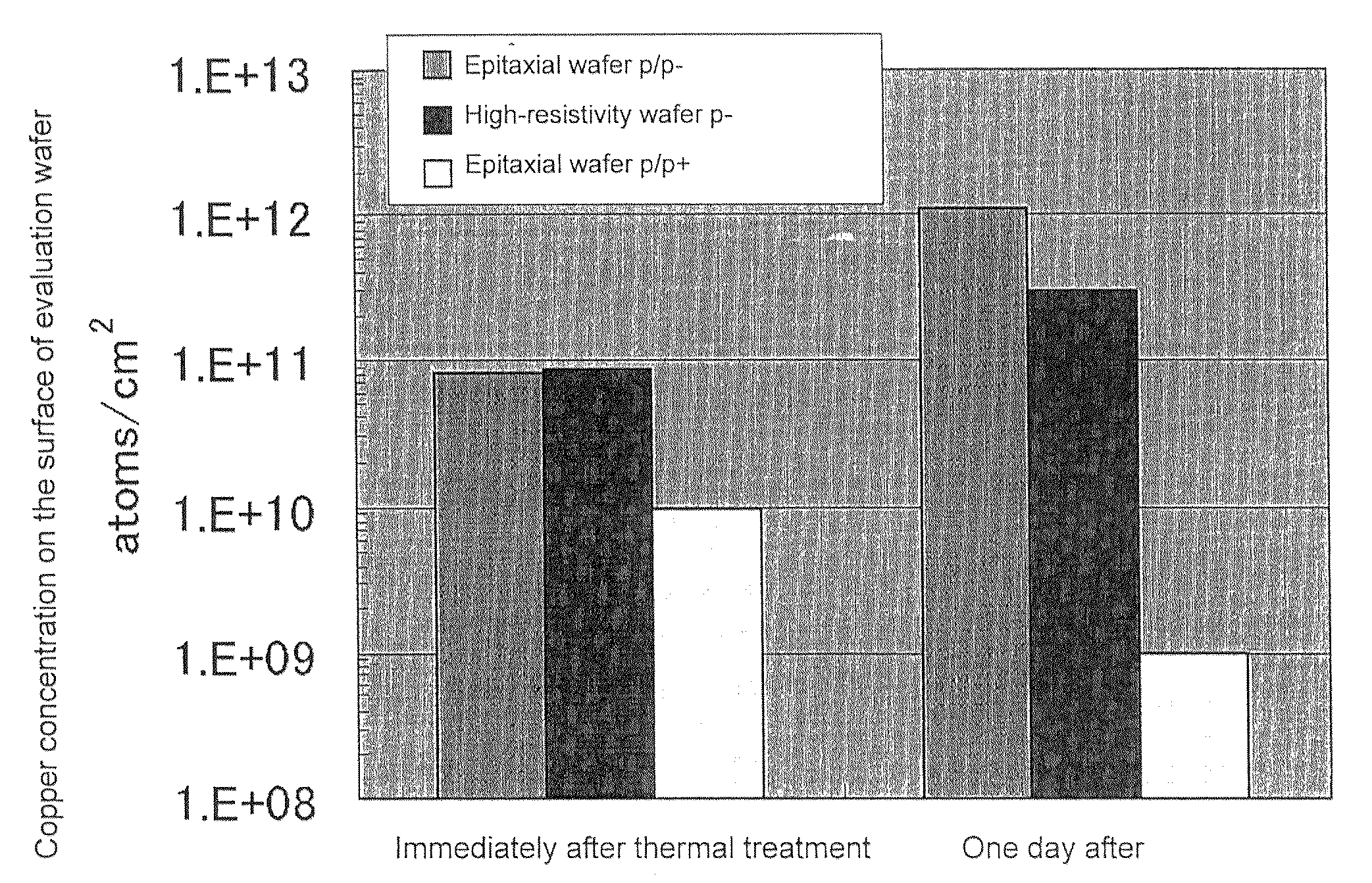
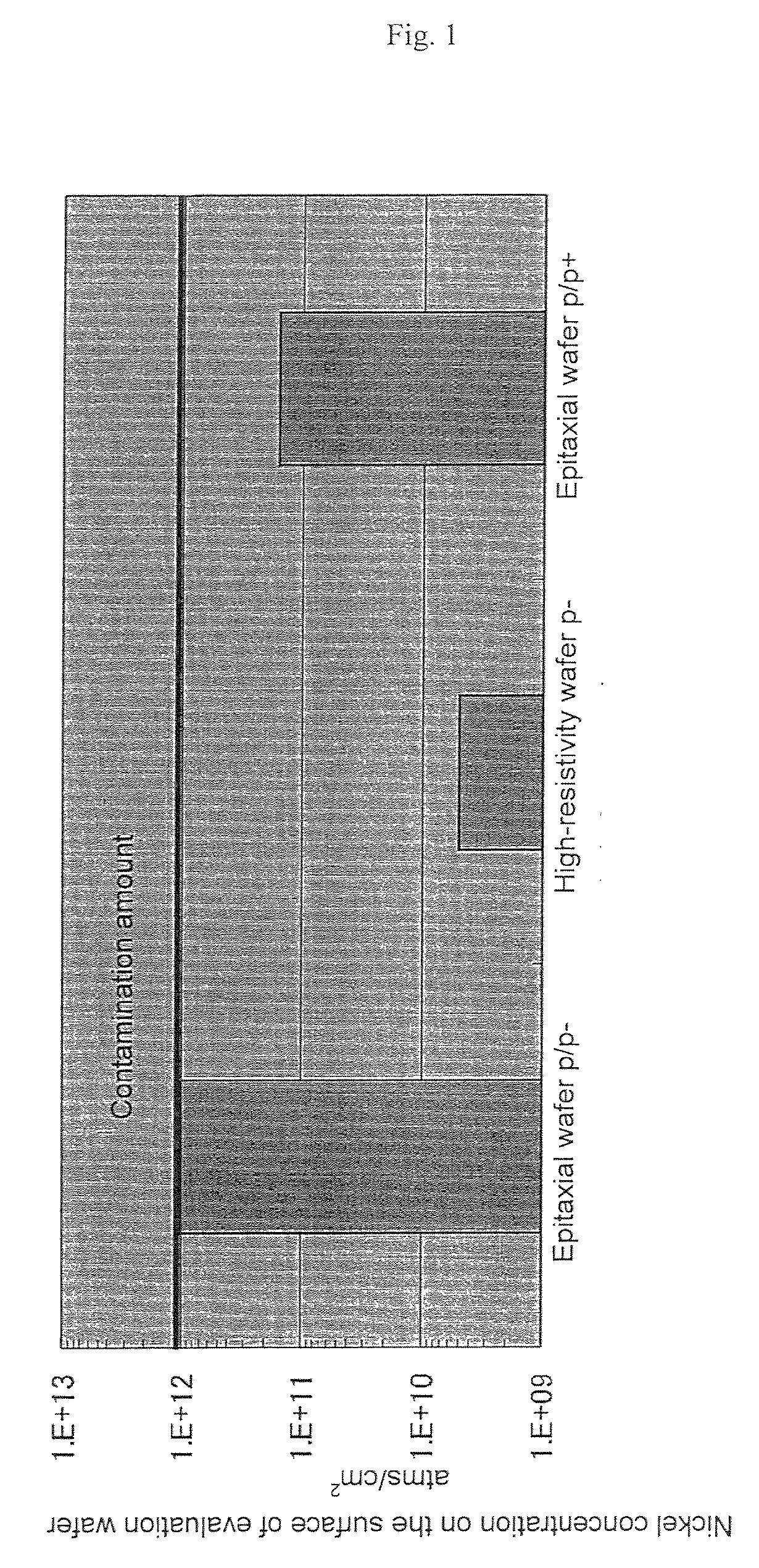
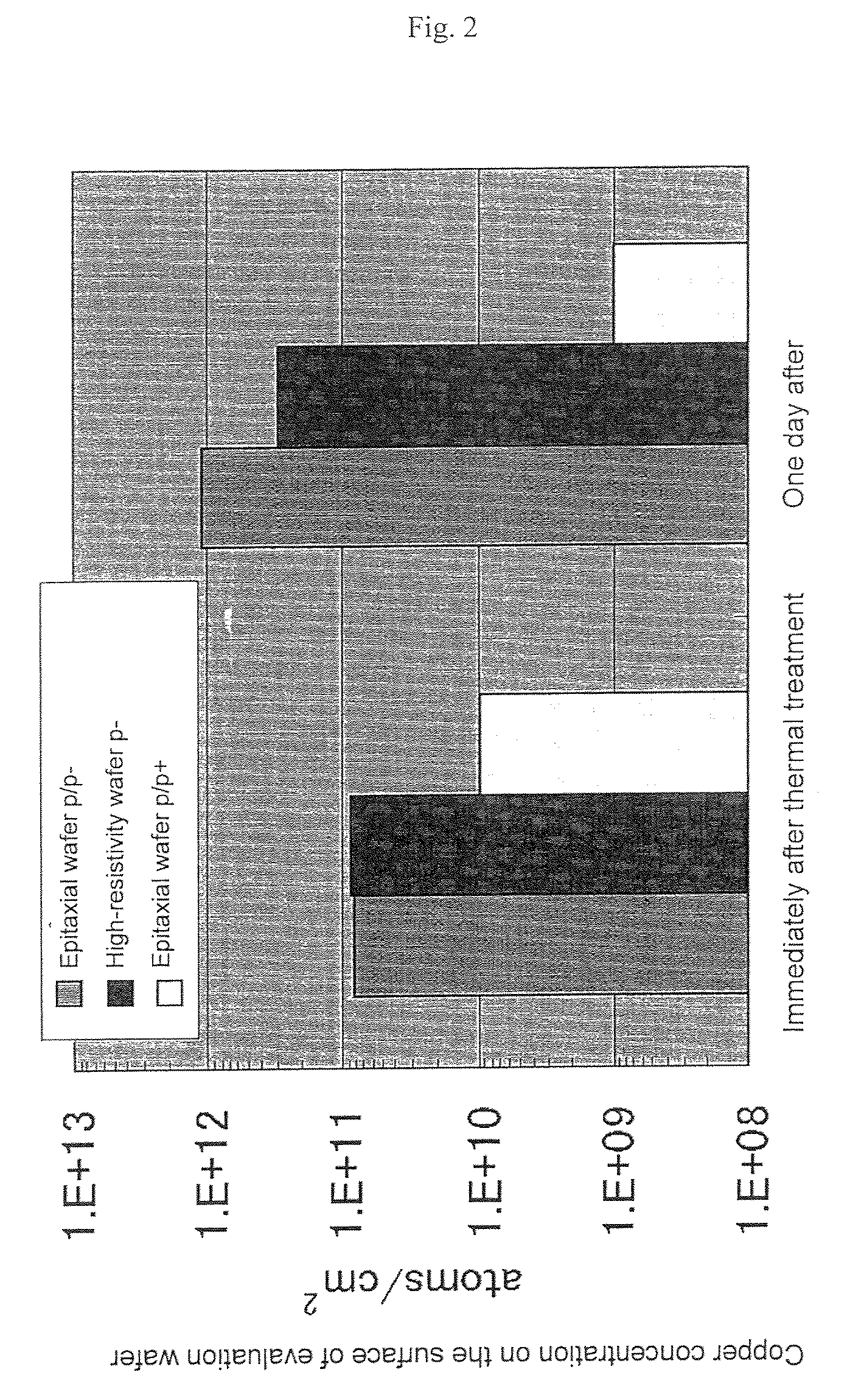
[0076] The above wafer was contaminated to a known nickel contamination level of 1×10¹² atoms / cm2 and heat treated to remove the surface oxide film. Subsequently, the nickel on the surface of the wafer was collected with an acidic collection solution (HF (2 weight percent) / H2O2 (2 weight percent) / H2O) and quantitatively analyzed by ICP-MS. Collection of the surface oxide film was conducted in the same manner as in Example 2 mentioned below.

[0077] As a comparative sample, the same treatment was conducted with a high-resistivity wafer (p−) and an epitaxial wafer (p / p+) having a substrate with low r...

example 2

Evaluation of Thermal Treatment Processes

(1) Analysis of Nickel

[0082] A boron-doped epitaxial layer (thickness: 3 micrometers; resistivity: 6 ohms·cm) was deposited on a boron-doped silicon substrate (oxygen concentration: 1.0×10¹⁸ atoms / cm3 (ASTM F-121 1979), resistivity: 4 ohms·cm) to prepare epitaxial wafers (p / p−) for evaluation of thermal treatment.

[0083] The above-described wafers for evaluation of thermal treatment were thermally treated under nitrogen atmospheres under one of the four conditions of 1 hour at 900 degrees Celsius, 10 hours at 900 degrees Celsius, 1 hour at 1,100 degrees Celsius, and 10 hours at 1,100 degrees Celsius in a heating furnace 1 employing a board treated with a CVD coating of SiC and a heating furnace 2 employing a board that had not been treated with a CVD coating of SiC.

[0084] Following thermal treatment, a hydrofluoric acid solution was introduced into a sealed container to remove the surface oxide films on the thermally treated wafers by va...


PUM

PropertyMeasurementUnit
thicknessaaaaaaaaaa
resistivityaaaaaaaaaa

Abstract

Provided are the methods of evaluating thermal treatment. In the methods, a wafer comprising a silicon substrate having an oxygen concentration of approximately equal to or less than 1.0×10¹⁸ atoms/cm3 and a silicon epitaxial layer on at least one surface of the substrate is employed.

Description

CROSS-REFERENCE TO RELATED APPLICATIONS [0001] This application claims benefit of priority under 35 USC 119 to Japanese Patent Application No. 2006-103845 filed on Apr. 5, 2006, which is expressly incorporated herein by reference in its entirety. BACKGROUND OF THE INVENTION [0002] 1. Field of the Invention [0003] The present invention relates to a method of evaluating thermal treatment that is capable of conveniently evaluating with high precision the metal contamination from a thermal treatment process in the process of manufacturing a semiconductor wafer; and a method of manufacturing a semiconductor wafer capable of providing a semiconductor wafer with less contamination by metals from a thermal treatment process. [0004] 2. Discussion of the Background [0005] Impurities in semiconductor wafers can compromise device characteristics and greatly affect device manufacturing yields. Among such impurities, metal impurities readily diffuse into the interior of wafers during various ther...

Claims


Application Information

Patent Timeline
Patent Type & Authority Applications(United States)
IPC IPC(8): H01L21/66
CPCH01L22/12
Inventor YAMASHITA, TAKAFUMISHABANI, MOHAMMAD B.
Owner SUMCO CORP
Why Eureka
Try Eureka