
Dual Damascene Copper Process Using a Selected Mask

Active Publication Date: 2008-01-24
SEMICON MFG INT (SHANGHAI) CORP
View PDF13 Cites 23 Cited by
  • Summary
  • Abstract
  • Description
  • Claims
  • Application Information

AI Technical Summary

Benefits of technology

[0011] Many benefits are achieved by way of the present invention over conventional techniques. For example, the present technique provides an easy to use process that relies upon conventional technology. In some embodiments, exemplary methods used reduce the number of required process steps by only utilizing one lithography step instead of two steps as required by a conventional dual damascene processes. Additionally, only a selected lithography mask is required as opposed to the two or more masks required in conventional dual damascene processes. In some embodiments, a reduced process time can be achieved by using fewer process steps, leading to cost savings and a reduced cycle time. Additionally, the method provides a process that is compatible with conventional process technology without substantial modifications to conventional equipment and processes. Depending upon the specific embodiment, one or more of these benefits may be achieved. These and other benefits will be described in more throughout the present specification and more particularly below.

Problems solved by technology

An IC fabrication facility can cost hundreds of millions, or even billions, of dollars.
Making devices smaller is very challenging, as each process used in IC fabrication has a limit.
However, one significant problem that has occurred with the increasing use of copper interconnects is that copper is a much more difficult material than aluminum to etch and pattern because it does not form a volatile byproduct.
Thus, copper metallization schemes cannot be used with conventional subtractive etching procedures used for aluminum.

Method used


Image

  • Dual Damascene Copper Process Using a Selected Mask
  • Dual Damascene Copper Process Using a Selected Mask
  • Dual Damascene Copper Process Using a Selected Mask

Examples


Embodiment Construction

[0019] The present invention is directed to integrated circuits and their processing for the manufacture of semiconductor devices. More particularly, the invention provides a novel method for a dual damascene process that uses a selected mask in the manufacture of integrated circuits. Merely by way of example, the invention can be applied to a copper metal damascene structure such as a dual damascene structure used for advanced signal processing devices. But it would be recognized that the invention has a much broader range of applicability. For example, the invention can be applied to microprocessor devices, logic circuits, application specific integrated circuit devices, as well as various other interconnect structures.

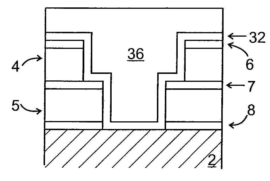
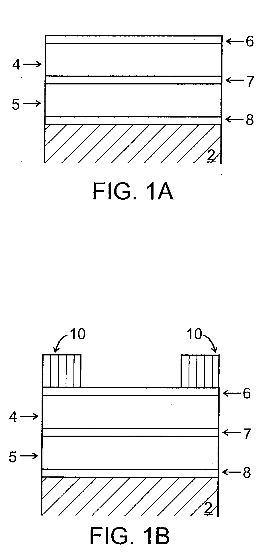
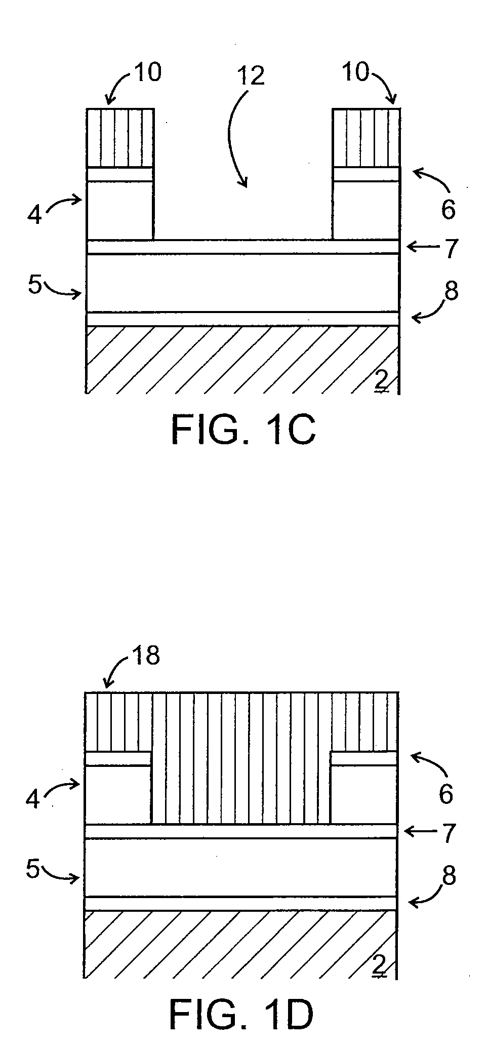
[0020]FIGS. 1A-1H are simplified cross-section views of layers overlying a surface region during a trench-first dual damascene process; In FIG. 1A, three layers of hard mask 6, 7, 8 and two layers of low-k dielectric 4, 5 overly copper line 2. Copper line 2 additio...


PUM


Abstract

A method for creating a dual damascene structure while using only one lithography and masking step. Conventional dual damascene structures utilize two lithography steps: one to mask and expose the via, and a second step to mask and expose the trench interconnection. The novel method for creating a dual damascene structure allows for a smaller number of processing steps, thus reducing the processing time needed to complete the dual damascene structure. In addition, a lower number of masks may be needed. The exemplary mask or reticle used within the process incorporates different regions possessing different transmission rates. During the exposing step, light from an exposing source passes through the mask to expose a portion of the photoresist layer on top of the wafer. Depending on the transmission rate of the different regions, different thickness of the photoresist layer are exposed and later removed by a developing solution, which allows a subsequent etch process to remove portions of both the dielectric layer and photoresist layer to create a dual damascene structure.

Description

CROSS-REFERENCES TO RELATED APPLICATIONS [0001] This application claims priority to Chinese Patent Application No. 200610023301.1, filed Jan. 13, 2006, commonly assigned, incorporated by reference herein for all purposes. BACKGROUND OF THE INVENTION [0002] The present invention is directed to integrated circuits and their processing for the manufacture of semiconductor devices. More particularly, the invention provides a novel method for a dual damascene process that uses a selected mask in the manufacture of integrated circuits. Merely by way of example, the invention can applied to a copper metal damascene structure such as a dual damascene structure used for advanced signal processing devices. But it would be recognized that the invention has a much broader range of applicability. For example, the invention can be applied to microprocessor devices, logic circuits, application specific integrated circuit devices, as well as various other interconnect structures. [0003] Integrated ...

Claims


Application Information

Patent Timeline
IPC IPC(8): H01L21/44G03F1/00
CPCG03F1/54H01L2221/1021H01L21/76807G03F1/50
Inventor TSENG, FAN CHUNGWU, CHI HSICHIEN, WEI TING
Owner SEMICON MFG INT (SHANGHAI) CORP
Features
  • Generate Ideas
  • Intellectual Property
  • Life Sciences
  • Materials
  • Tech Scout
  • Unparalleled Data Quality
  • Higher Quality Content
  • 60% Fewer Hallucinations
Learn More