Method of designing semiconductor integrated circuit, designing apparatus, semiconductor integrated circuit system, semiconductor integrated circuit mounting substrate, package and semiconductor integrated circuit

Inactive Publication Date: 2008-01-24
SOCIONEXT INC
View PDF5 Cites 9 Cited by
  • Summary
  • Abstract
  • Description
  • Claims
  • Application Information

AI Technical Summary

Benefits of technology

[0014] In consideration of the actual conditions, it is an object of the invention to provide a semiconductor integrated circuit system which can design a semiconductor integrated circuit, a package and a mounting substrate with a high workability also in an increase in a scale and an integration of an LSI, can reduce an unnecessary radiation and is excellent in a heat characteristic.

Problems solved by technology

On the other hand, however, there is a problem in that an unnecessary radiation generated from these products causes a radio interference of a receiving device such as a television or a radio and a malfunction of other systems.
However, it is hard to take the countermeasure in respect of an increase in the number of components, an increase in a cost and the difficulty of a countermeasure to be taken against the product.
Therefore, a consideration cannot be taken and there is a drawback that an intersection of the wiring on the package substrate is caused and a wiring length is increased.
For this reason, it is also hard to carry out a design without a feedback.
There is a problem in that a circuit design of the LSI becomes complicated, and furthermore, the number of external connecting terminals is increased and it is hard to correspond to a change into a multibit with the increase in the scale and integration of the LSI.
Moreover, an arrangement of a signal wiring becomes complicated.
For this reason, there is also a problem in that an unnecessary radiation (EMI) analysis and a thermal analysis become complicated, and it is hard to carry out a perfect automation in an optimization of the design, and a manual correction is required, resulting in an increase in a time required for a development.

Method used


Image

  • Method of designing semiconductor integrated circuit, designing apparatus, semiconductor integrated circuit system, semiconductor integrated circuit mounting substrate, package and semiconductor integrated circuit
  • Method of designing semiconductor integrated circuit, designing apparatus, semiconductor integrated circuit system, semiconductor integrated circuit mounting substrate, package and semiconductor integrated circuit
  • Method of designing semiconductor integrated circuit, designing apparatus, semiconductor integrated circuit system, semiconductor integrated circuit mounting substrate, package and semiconductor integrated circuit

Examples


first embodiment

[0166] Prior to explanation of the embodiments according to the invention, description will be first given to a concept of the invention.

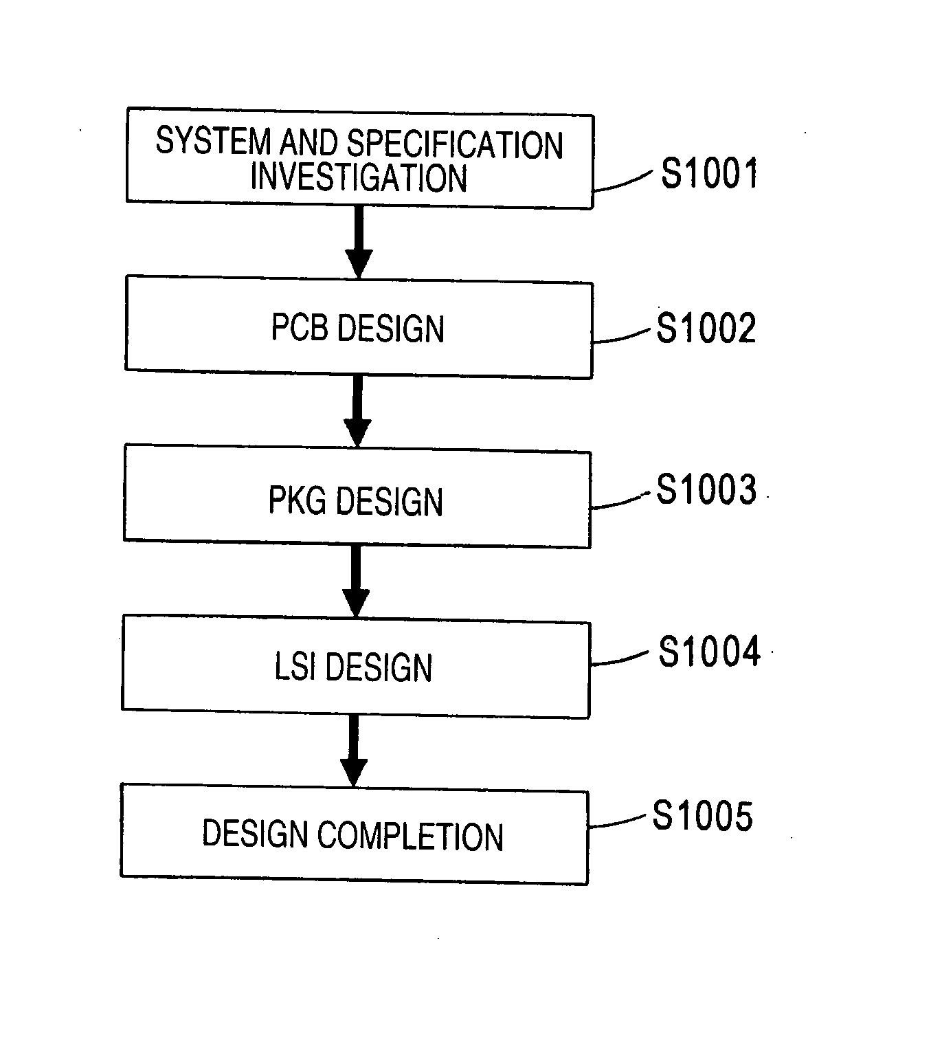
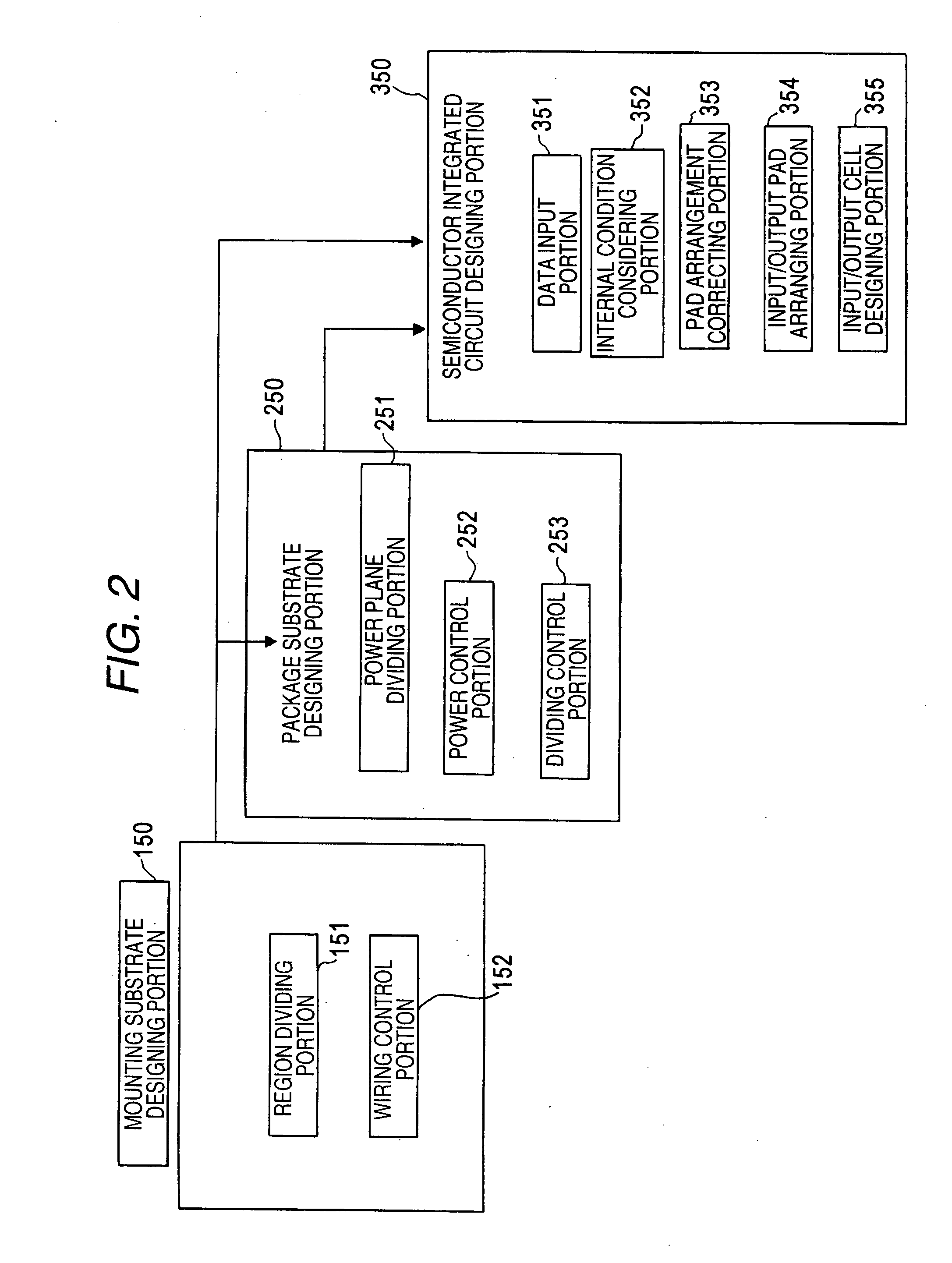
[0167]FIG. 1 is an explanatory diagram showing a design flow and FIG. 2 shows an apparatus for designing a semiconductor integrated circuit system. In the embodiment, a system specification including, on a printed wiring board, a semiconductor integrated circuit (LSI) to be accommodated in a package and other electronic components such as a memory is investigated (system and specification investigation: Step 1001), the printed wiring board is designed based on information about a component arrangement on the printed wiring board (a design of the printed wiring board: Step 1002). Then, a position of a ball to be an external connecting terminal on a package substrate constituting a package is investigated based on the information about a component arrangement on the printed wiring board and the package is designed in consideration of a signal wiring...

second embodiment

[0220] Next, description will be given to a method of designing a package according to a second embodiment of the invention.

[0221] For the package, there have been proposed various packages using a lead frame and a film carrier. Herein, there will be utilized a package having a ball grid array structure using a multilayered structure substrate as a package substrate and using a ball as an external connecting terminal.

[0222] While the method of designing a printed wiring board to mount a package substrate mounting a semiconductor integrated circuit chip has been described in the first embodiment, description will be given to a method of designing a package substrate to be used in the embodiment.

[0223] As shown in a schematic sectional view of FIG. 15, the package is constituted by a package substrate 201 having a four-layer structure including a surface layer 201a having a surface layer wiring, a power layer 201b constituting a power plane, a ground layer 201c constituting a groun...

third embodiment

[0245] Next, description will be given to a third embodiment according to the invention.

[0246] The method is characterized in that a plane of a package substrate is divided into four regions and a signal wiring is completed for each of the regions in a design of the package substrate.

[0247]FIG. 20 is a flowchart showing a method of designing a package according to the embodiment, and particularly, a method of designing an in-region wiring thereof. FIG. 21 is an explanatory view showing the designing method.

[0248] In the method, first of all, a size, a shape and a ball arrangement of a ball (a ball grid array) to be an external connecting terminal of a package substrate 200 and a size and a pad arrangement of an LSI 300 are superposed as input information, and superposition data are output as shown in FIG. 21(a) (Step 1021).

[0249] Then, a thickness and a length of a wire W and a bond finger BF are set to be input information in addition to the superposition data, and the ball 202...


PUM


Abstract

To provide a method of designing a semiconductor integrated circuit with a high workability also in an increase in a scale of an LSI and an enhancement in an integration and designing a semiconductor integrated circuit system in which an unnecessary radiation is reduced and which is excellent in a heat characteristic, a reverse design flow to that in the conventional art is implemented, and a mounting substrate such as a printed-circuit board is first designed and a package substrate for mounting an LSI is designed based on a result of the design of the mounting substrate, and a layout design of the LSI to be mounted on the package substrate is then carried out.

Description

BACKGROUND OF THE INVENTION [0001] 1. Field of the Invention [0002] The present invention relates to a method of designing a semiconductor integrated circuit, a designing apparatus, a semiconductor integrated circuit system, a semiconductor integrated circuit mounting substrate, a package and a semiconductor integrated circuit, and more particularly to a method of designing a semiconductor integrated circuit system which designs a semiconductor integrated circuit and reduces an unnecessary radiation (EMI: Electromagnetic Interference), and furthermore, is excellent in a heat characteristic in consideration of a mounting state based on a result of a design of a mounting substrate constituting the semiconductor integrated circuit system. [0003] 2. Description of the Related Art [0004] A semiconductor integrated circuit (LSI) has a utilization range enlarged to communicating apparatuses such as a cell phone, general domestic articles, toys and cars in addition to a computer. On the oth...

Claims


Application Information

Patent Timeline
IPC IPC(8): G06F17/50H01L23/48
CPCG06F17/5068H01L23/49838H01L2924/12041H01L2924/01087H01L2924/01019H01L2924/01006H01L24/48H01L2924/3025H01L23/50H01L24/49H01L2224/48091H01L2224/48227H01L2224/48235H01L2224/49112H01L2224/49171H01L2924/01002H01L2924/01004H01L2924/01005H01L2924/01013H01L2924/01015H01L2924/01029H01L2924/01033H01L2924/01056H01L2924/01057H01L2924/01074H01L2924/01075H01L2924/01082H01L2924/14H01L2924/15311H01L2924/19041H01L2924/19042H01L2924/19043H01L2924/30105H01L2924/30107H01L2924/3011H01L2924/00014H01L2924/00G06F30/39H01L2224/05554H01L2224/45099H01L2224/05599
Inventor TOKUNAGA, SHINYAITO, MITSUMIIWANISHI, NOBUFUSASEKO, KOICHISUZUKI, HIROAKITANAKA, HIROYUKINISHIMURA, YUICHIFUJIMOTO, KAZUHIKO
Owner SOCIONEXT INC
Why Eureka
Try Eureka