Substrate and process for semiconductor flip chip package

a technology of semiconductor flip chip and substrate, which is applied in the direction of sustainable manufacturing/processing, printed circuit aspects, final product manufacturing, etc., can solve the problems of non-uniform size of bumps, elevation offset problems, and no verdict on this matter one way, so as to improve yield and package reliability, the effect of improving the reliability of the sock

Active Publication Date: 2008-01-31
INTELLECTUAL VENTURES FUND 27
View PDF6 Cites 40 Cited by
  • Summary
  • Abstract
  • Description
  • Claims
  • Application Information

AI Technical Summary

Benefits of technology

[0013]According to an illustrative embodiment of the present invention, the etching holes are filled with solder paste. The chip is studd|[.1] bumpedstud or bumped with other technique. The flip chip package is formed by having the bumps on the chip penetrate into the etching holes filled with solder paste. Therefore, after a reflow process, the contact area between the bumps and the bump pads is not li...

Problems solved by technology

As a result, there is no verdict on this matter one way or another.
Such bump to bump pad connection method suffers from several problems when there are defects or alignment problems on the chip 120...

Method used


Image

  • Substrate and process for semiconductor flip chip package
  • Substrate and process for semiconductor flip chip package
  • Substrate and process for semiconductor flip chip package

Examples


Embodiment Construction

[0032]Various embodiments will be described in detail with reference to the drawings, wherein like reference numerals represent like parts and assemblies throughout the several views. Reference to various embodiments does not limit the scope of the claims attached hereto. Additionally, any examples set forth in this specification are not intended to be limiting and merely set forth some of the many possible embodiments for the appended claims.

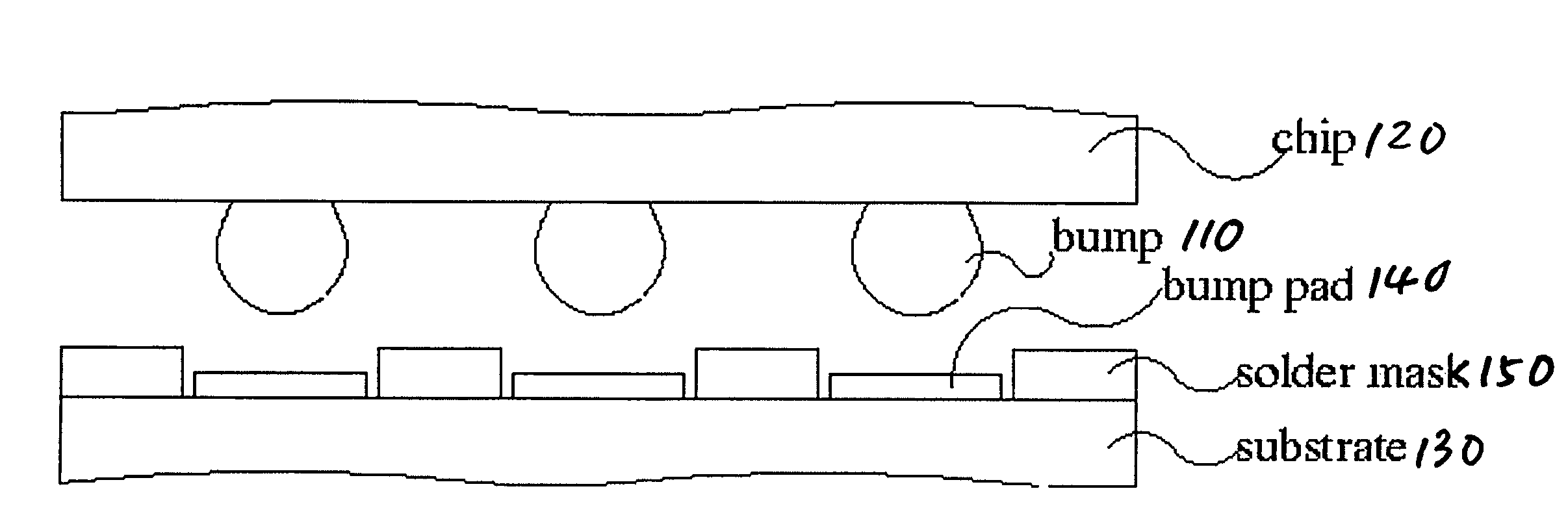
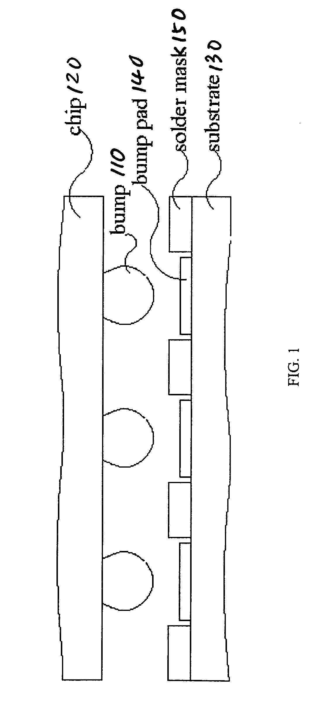
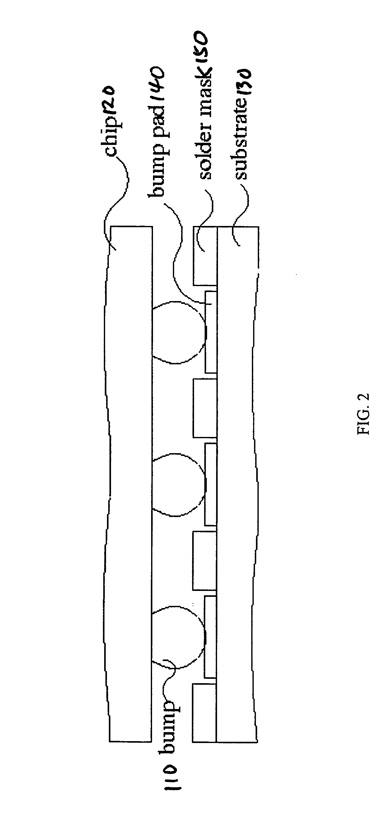
[0033]This application discloses a new way to form electrical connection between the bumped chip and the patterned circuit layer of the substrate. As will be discussed regarding the illustrative embodiments of the present invention, most of the fabrication problem in flip chip can be relieved by using a simple process discussed in this invention.

[0034]FIG. 8 is a cross-sectional view of disclosed flip chip substrate taking copper as an example to form the patterned circuit layer according to an illustrative embodiment of the invention. As shown...


PUM


Abstract

A semiconductor package structure for flip chip package includes at least a patterned circuit layer and an insulating layer alternately stacking up each other. The patterned layer includes a plurality of bump pads, and the insulating layer includes a plurality of etching holes. The etching holes and the bump pads are aligned, such that the bump pads are exposed through the etching holes. A plurality of bumps is disposed on the active surface of the chip, which can be obtained by stud bumping. The etching holes are filled with solder paste, and the bumps of the chips penetrate into the solder filled etching holes. Vibration obtained by mechanical equipment, or ultrasonic equipment can be applied to assist the alignment of the bumps to the corresponding bump pads. A reflow process is applied to collapse the solder paste that fills the etching holes to form electrical connection between the bumps and bump pads.

Description

BACKGROUND OF THE INVENTION[0001]This invention relates to a substrate for semiconductor flip chip package, and a process to fabricate the flip chip device with the substrate.[0002]Flip chip technology is one of the most frequently used package technology for chip scale package. As the flip chip technology can employ area array to dispose bump pad and be connected to the carrier through a bump, it can reduce the packaging area and shorten the transmission path of the signal. Traditional type of bump pad design of the substrate can be classified into SMD (Solder Mask Defined) type and NSMD (Non-Solder Mask Defined) type. Each of these two types of bump pad design has its own merits and demerits. As a result, there is no verdict on this matter one way or another.[0003]FIGS. 1 and 2 are cross-sectional views of a flip chip package of the NSMD type as an example in the prior art. As shown in FIGS. 1 and 2, a plurality of bumps 110 is formed on the active surface of the chip 120. The chi...

Claims


Application Information

Patent Timeline
IPC IPC(8): H01L23/48
CPCH01L23/142H01L23/49822H01L24/13H01L2224/1403H01L2224/16237H01L24/10H01L24/81H01L24/83H01L24/90H01L2224/13099H01L2224/16225H01L2224/81136H01L2224/8121H01L2224/81815H01L2224/838H01L2924/01005H01L2924/01027H01L2924/01029H01L2924/01033H01L2924/01046H01L2924/01047H01L2924/01078H01L2924/01079H01L2924/01082H05K3/3436H05K3/3452H05K3/3484H05K2201/09427H05K2201/09472H05K2201/09509H01L2924/01006H01L2924/0105H01L2924/01067H01L2924/01087H01L2924/014H01L2924/3512H01L2924/00H01L24/16H01L2224/81191H01L2924/00011H01L2924/00014H01L2924/351H05K3/3485Y02P70/50H01L2224/0401H01L21/56H01L23/498H05K3/34
Inventor KOK, CHI WAHTAM, YEE CHING
Owner INTELLECTUAL VENTURES FUND 27
Why Eureka
Try Eureka