Optical modulator

a modulator and optical technology, applied in optics, instruments, optical light guides, etc., can solve the problems of difficult to separate primary mode light from signal light, and achieve the effects of reducing the thickness of substrate, enhancing the confinement of light into the substrate, and reducing the loss of curving optical waveguides

Active Publication Date: 2008-01-31
NGK INSULATORS LTD
View PDF17 Cites 18 Cited by
  • Summary
  • Abstract
  • Description
  • Claims
  • Application Information

AI Technical Summary

Benefits of technology

[0014] The present inventors found that, as the substrate thickness is reduced, confinement of light into the substrate is enhanced due to the presence of a low-dielectric constant layer or air layer in the thickness direction, so that the curving loss of the optical waveguide can be extremely reduced. For example, FIG. 6 shows the calculation results of optical loss of primary mode light to LN substrate thickness at a wavelength of 1.55 μm and a curvature radius of waveguide of 5 mm. It was found from the results that, even if the optical waveguide is curved, the optical loss can be reduced to 10 dB or less which is an unthinkable level in actual operation when the substrate thickness is 20 μm or less. It was also found that increase in curvature radius of the optical waveguide allows further reduction in the loss, and the optical loss can be reduced to 10 dB or less when the substrate thickness is 10 μm even in the case having a curvature radius of 1 mm.
[0015] The present inventors have simulated based on such knowledge to provide a guiding waveguide for propagating the primary mode light in the vicinity of a multiplexing part of a three-dimensional optical waveguide for propagating signal light so that the primary mode light is propagated separately from the signal light. Consequently, they found that operational point of the optical modulator can be easily controlled by considerably separating the light receiving point of the primary mode light from the light receiving point of the signal light from the above-mentioned reasons. The present invention is thus attained.

Problems solved by technology

However, the peak-to-peak distance of the primary mode light is 10 μm to 100 μm or less to signal light, and this makes it difficult to take out the primary mode light as monitor light separately from the signal light.

Method used


Image

  • Optical modulator
  • Optical modulator
  • Optical modulator

Examples


example 1

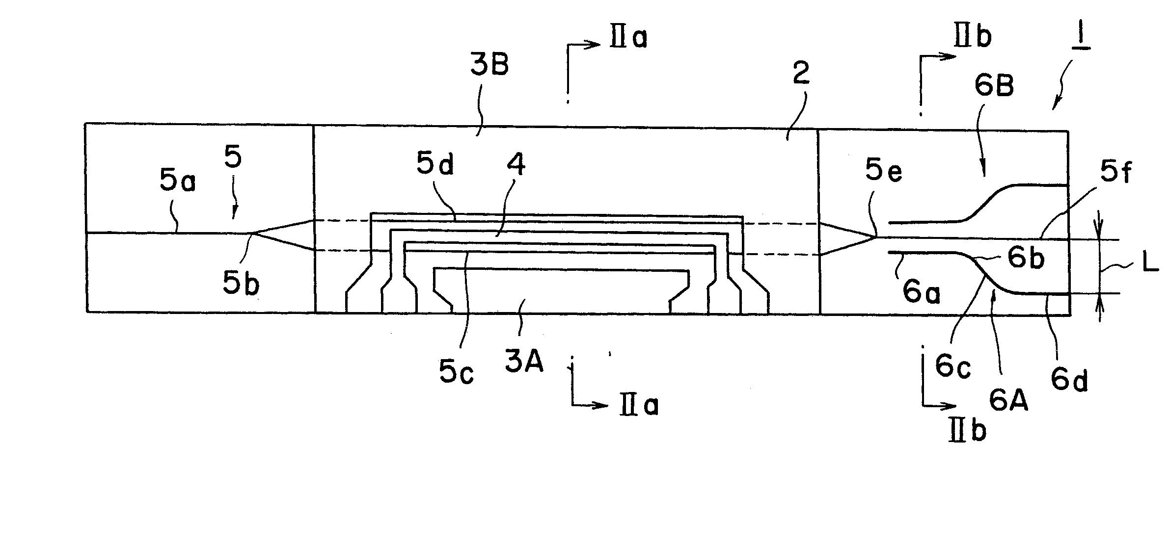
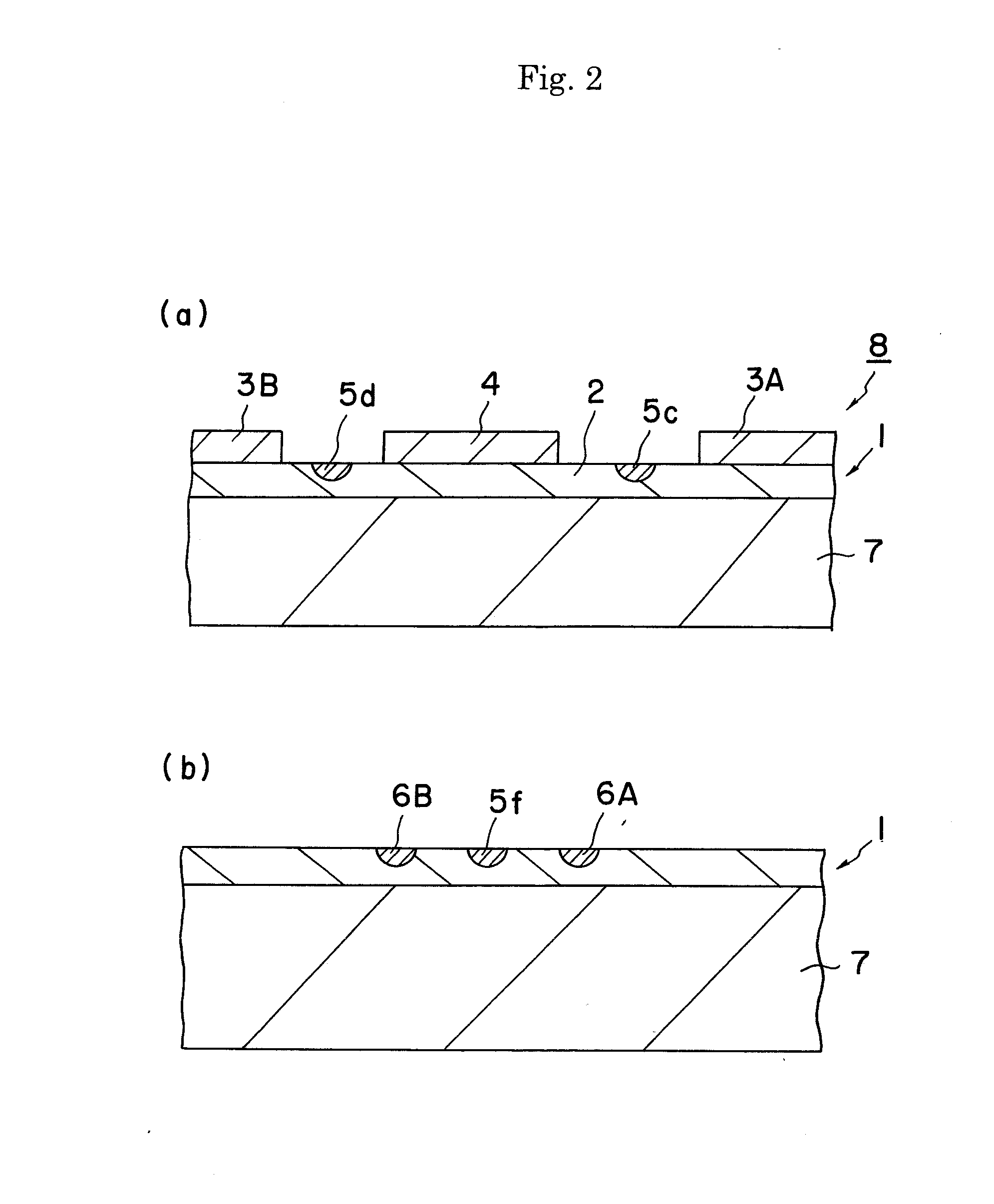
[0052] The optical modulator 1 of FIG. 1 was manufactured according to the method described in reference to FIGS. 1 to 3 and tested. Concretely, a substrate consisting of an X-cut 3-inch wafer (LiNbO3 single crystal) is used, and a Mach-Zehnder optical waveguide 5 is formed on a surface of the wafer by titanium diffusion process and photolithography. A CPW electrode is formed by plating process. The gap of a central electrode 4 to ground electrodes 3A and 3C is 25 μm, the electrode thickness is 20 μm, and the electrode length is 32 mm. A grinding dummy substrate is stuck to a grinding surface plate for thinning grinding, and the modulator substrate is stuck thereto through a thermoplastic resin with the electrode surface down. Further, the substrate body is thinned to a thickness of 8 μm by horizontal grinding and polishing (CMP). Thereafter, the flat plate-like support substrate 7 is adhered and fixed to the substrate body, and a connection part for an optical fiber is end surface-...

example 2

[0054] Investigation was performed for the optical modulator described in reference to FIGS. 4 and 5.

[0055] Concretely, the material of the optical modulator and the forming method of the optical waveguide are the same as in the Example 1. In a photodiode having a light receiving area of 50 μm, Wti-m was set to 30 μm in consideration of spread. The curvature radius r of the curved part of the guiding waveguide was set to 5 mm. The substrate thickness of the optical modulator was changed as shown in FIG. 6 with λ of 1.55 μm. FIG. 11 shows the planar positional relation of the guide waveguide and the emission part 5f. The distance Sx between the edge of each guide waveguide and the central axis of the emission part is 20 μm.

[0056] The optical loss of off-light (primary mode light) was measured while changing the thickness Tsub of the substrate in this state. Consequently, the results shown in FIG. 6 were obtained. Namely, it was found that when the thickness of the substrate is 20 μ...

example 3

[0057] The optical loss of the primary mode light propagating in the guiding waveguide was tested in the same manner as in the Example 2. In this example, λ is 1.55 μm, the substrate thickness Tsub of the optical modulator is 8 μm, titanium thickness Tti is 600 Å, the width Wti of the signal light emission part is 5 μm, and the width Wti-m of the guiding waveguide is 30 μm. The distance Sx between the edge of the guiding waveguide and the central axis of the emission part and the curvature radius r of the curved part of the guiding waveguide were changed as shown in FIG. 7.

[0058] As a result, the optical loss at R of 20 μm or less was suppressed to 10 dB or less. Even if Sx is variously changed between 10 μm and 100 μm, the optical loss in the guiding waveguide was not substantially increased.


PUM

PropertyMeasurementUnit
thicknessaaaaaaaaaa
distanceaaaaaaaaaa
widthaaaaaaaaaa

Abstract

An optical modulator is provided for modulating light propagating in a three-dimensional optical waveguide 5 by applying a voltage thereto. The optical modulator has the three-dimensional optical waveguide 5 including at least one pair of branch optical waveguides 5c and 5d, a multiplexing part 5e of the branch optical waveguides and an emission part 5f provided in the downstream of the multiplexing part, modulation electrodes 3A, 3B and 4 for applying a signal voltage for modulating light propagating in the three-dimensional optical waveguide 5, and guiding waveguides 6A and 6B for guiding primary mode light from the multiplexing part. Thickness of the substrate is 20 μm or less at least under the modulation electrodes, and an operation point of the optical modulator is controlled by changing, based on light output from the guiding waveguides, DC bias applied onto the modulation electrodes.

Description

FIELD OF THE INVENTION [0001] The present invention relates to an optical modulator using a so-called Mach-Zehnder optical waveguide. BACKGROUND OF THE INVENTION [0002] A traveling-wave high-speed optical modulator using a Mach-Zehnder optical waveguide has drawn attention due to its wide wavelength band and low chirp characteristic. This type of optical modulators is adapted to propagate light in a pair of branch optical waveguides, respectively, and merge output from each branch optical waveguide together in its multiplexing part. However, shift of operational point and so-called DC drift may be caused between the pair of branch optical waveguides due to a temperature difference or the like. A Mach-Zehnder (MZ) LN optical modulator generally involves the shift of operational point caused by temperature drift, DC drift, stress by a change with time or the like, resulting in a deterioration of extinction ratio. This problem is important in operation of the modulator. [0003] Several ...

Claims


Application Information

Patent Timeline
Patent Type & Authority Applications(United States)
IPC IPC(8): G02F1/295
CPCG02F1/0123G02F1/2255G02F2203/20G02F2201/58G02F2001/212G02F1/212
Inventor KONDO, JUNGOMITOMI, OSAMUAOKI, KENJIIWATA, YUICHIEJIRI, TETSUYA
Owner NGK INSULATORS LTD
Why Eureka
Try Eureka