Systems and methods for optimizing the crystallization of amorphous silicon

a technology of amorphous silicon and crystallization method, which is applied in the field of systems and methods for manufacturing lcds, can solve the problems of high process operational cost, low productivity of a-si technology, and approaching its limitations, and achieve the effect of improving the uniformity of transistors made in the material

Inactive Publication Date: 2008-02-07
TCZ
View PDF8 Cites 14 Cited by
  • Summary
  • Abstract
  • Description
  • Claims
  • Application Information

AI Technical Summary

Benefits of technology

[0021]A thin beam directional crystallization system configured to anneal a silicon layer on a glass substrate can, in one embodiment, use a special short-axis laser beam profile that included an intensity peak at one edge. In another embodiment epitaxial lateral growth can be terminated at predetermined locations such that, upon the continuation of the process, epitaxial growth is re-initiated from new seeds. Thus, the crystallographic orientation of the growing grains can be randomized. Because the epitaxial lateral growth is stopped and restarted, e.g., less than every 20 micrometers or so, there will be less opportunity for texture to develop within the crystallized film. Thus uniformity of transistors made in the material can be improved.

Problems solved by technology

This is due primarily to the relatively lower costs of a-Si that result from fewer process steps and the potential unknowns associated with less mature LTPS equipment.
A-Si also has been a “safe” process for minimizing costs, since a single defect in a large screen LCD means scrapping the whole device; however, even though a-Si processes are fairly well established and controllable, it has now become clear that a-Si technology is approaching its limitations with regard to supporting the emerging demand for higher pixel densities, faster response, and brighter displays.
The primary challenges in LTPS technologies involve the effective control of the process to assure uniform crystallization across the entire panel while providing a high level of sustained process throughput and low operational costs.
Low productivity and high operational expenses of the process have hampered the wide adoption of ELA.
From a performance and yield perspective, the ELA process has other significant limitations.
In addition, electron mobility is relatively low due to the small grain size, so the ELA process struggles to meet the requirements for System On Glass (SOG).
However, since the SLS mask is incrementally “stepped” to cover the panel in multiple passes, shot-to-shot variation in laser energy can lead to variability in the poly-Si throughout the panel.
Further, an unwanted artifact of the standard SLS technique is the large vertical protrusions that are formed during the solidification of the Silicon.
The pattern of protrusions that appear after SLS annealing can make it difficult to deposit a uniform gate dielectric layer, leading to non-uniformity in the TFT performance across the panel.
A smaller step size reduces throughput and increases costs.

Method used


Image

  • Systems and methods for optimizing the crystallization of amorphous silicon
  • Systems and methods for optimizing the crystallization of amorphous silicon
  • Systems and methods for optimizing the crystallization of amorphous silicon

Examples


Embodiment Construction

.”

BRIEF DESCRIPTION OF THE FIGURES

[0025]Features, aspects, and embodiments of the inventions are described in conjunction with the attached drawings, in which:

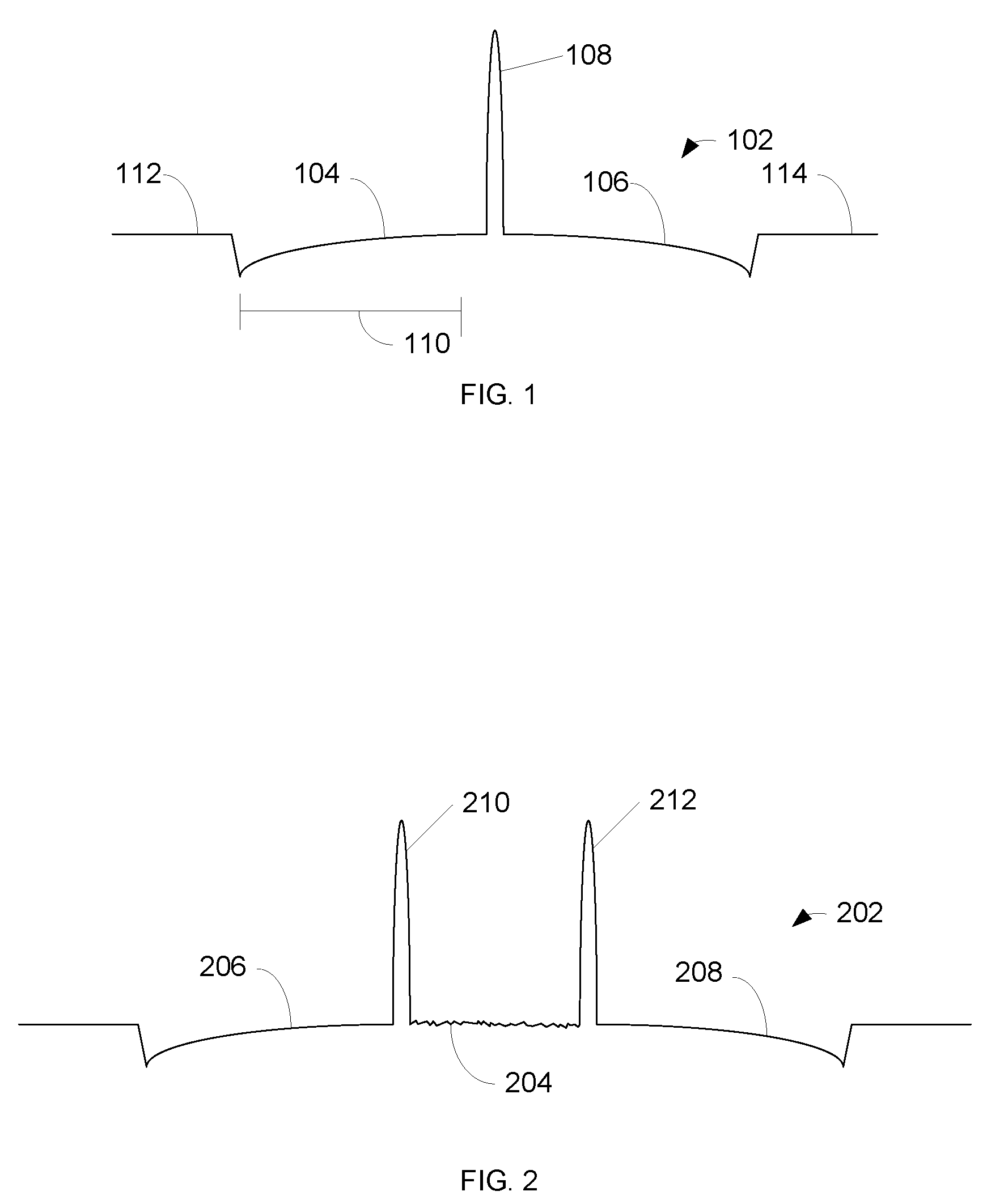
[0026]FIG. 1 is a diagram illustrating an example cross section of a film surface after a single pulse irradiation;

[0027]FIG. 2 is a diagram illustrating another example cross section of a film surface after a single pulse irradiation;

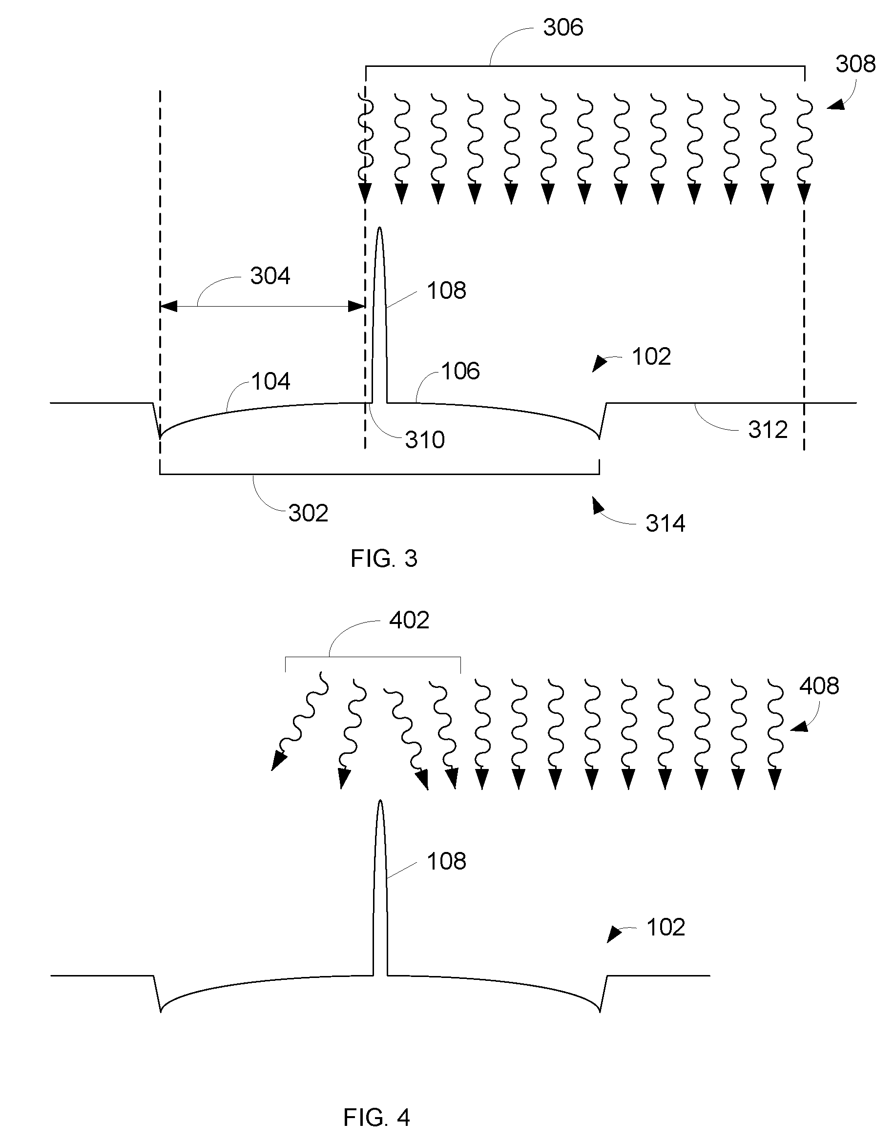
[0028]FIG. 3 is a diagram illustrating an example position of a beam during a second irradiation of the cross section of a film surface of FIG. 1;

[0029]FIG. 4 is a diagram illustrating an example scattering of incident photons during the second irradiation illustrated in FIG. 3;

[0030]FIGS. 5A-5C are diagrams illustrating example short-axis spatial intensity profiles;

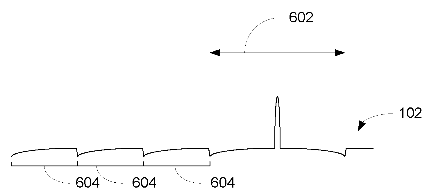
[0031]FIG. 6 is a diagram illustrating an example position of a film after “n” pulses;

[0032]FIG. 7 is a diagram illustrating a beam spatial intensity and an example position of a beam after “n+1” pulses;

[0033]FIG. 8 is an example devi...


PUM

PropertyMeasurementUnit
step sizeaaaaaaaaaa
step sizeaaaaaaaaaa
wavelengthsaaaaaaaaaa

Abstract

In a thin beam directional Crystallization System configured anneal a silicon layer on a glass substrate uses a special laser beam profile with an intensity peak at one edge. The system is configured to entirely melt a spatially controlled portion of a silicon layer causing lateral crystal growth. By advancing the substrate or laser a certain step size and subjecting the silicon layer to successive “shots” from the laser, the entire silicon layer is crystallized. The lateral crystal growth creates a protrusion in the center of the melt area. This protrusion must be re-melted. Accordingly, the step size must be such that there is sufficient overlap between successive shots, i.e., melt zones, to ensure the protrusion is melted. This requires the step size to be less than half the beam width. A smaller step size reduces throughput and increases costs. The special laser profile used in accordance with the systems and methods described herein can increase the step size and thereby increase throughput and reduce costs.

Description

BACKGROUND[0001]1. Field of the Invention[0002]The field of the invention relates generally to, Liquid Crystal Displays (LCDs), and more particularly to systems and methods for manufacturing LCDs.[0003]2. Background of the Invention[0004]There is already a well-established and growing market for active matrix LCDs, in which an active thin film transistor (TFT) is used to control each pixel in the display. For example, active matrix LCDs are the prevailing technology for computer screens. Additionally, in recent years, active matrix LCD solutions also have made dramatic inroads in market segments such as televisions, mobile phones, PDAs, video recorders, etc.[0005]Active matrix LCDs are predicted to be the fastest growing segment of the display industry, with a projected average annual growth rate of 35 percent over the next five years. In contrast, passive LCDs and conventional cathode ray tubes (CRTs), are predicted to have flat to negative growth rates. The only other display tech...

Claims


Application Information

Patent Timeline
Patent Type & Authority Applications(United States)
IPC IPC(8): G02B3/02
CPCB23K26/063B23K26/0732B23K26/0738B23K26/0853C30B13/24H01L21/02691G03F7/70383H01L21/02532H01L21/02678H01L21/02686C30B29/06B23K26/0622C30B35/00H01L21/324
Inventor TURK, BRANDON A.BURFEINDT, BERNDKNOWLES, DAVID S.
Owner TCZ
Why Eureka
Try Eureka