Dynamic memory refresh configurations and leakage control methods

a dynamic memory and refresh configuration technology, applied in static storage, information storage, digital storage, etc., can solve the problems of low factory yield, insufficient retention time, and certain portion of memory storage cells that do not function properly, so as to reduce power switching losses within dynamic memory, enhance dynamic memory characteristics, and reduce leakage

Inactive Publication Date: 2008-02-07
ZMOS TECH
View PDF4 Cites 80 Cited by
  • Summary
  • Abstract
  • Description
  • Claims
  • Application Information

AI Technical Summary

Benefits of technology

[0018] Circuits and methods are described for enhancing dynamic memory characteristics in response to the use of power source transistors, altering the refresh configuration and / or controlling circuit and cell leakage. At least one implementation describes the use of a burst mode refresh means which reduces power switching losses within dynamic memory. At least one implementation describes a means for reducing leakage arising from micro-bridging between bit and word-lines with current limiting means and fuse means. At least one implementation describes reducing unit cell leakage in response to adapting bit-line voltage profiles. At least one implementation describes a means for improving self refresh characteristics of those memory cells having a data retention time that is shorter than other memory cells by storing its address information in unused programmable fuses for redundant cells and altering its refresh period.
[0019] An example of the invention is a dynamic random access memory circuit (DRAM), comprising: (a) a plurality of memory cells configured for retaining cell data in response to the level of stored charge; (b) a plurality of bit-lines and word-lines coupled to the plurality of memory cells for accessing cell data; (c) a refresh circuit configured for grouping refresh cycles into a portion of the retention period; (d) a power control circuit configured for generating a power control signal for deactivating power when the memory circuit is not being accessed; and (e) the power control circuit configured for generating an active power level while the grouping of refresh cycles is being performed. As a result, the power control signal is not switched on and off for each refresh cycle within the retention period, thus reducing power consumption, such as in response to lowered capacitive charging and discharging.
[0020] The refresh cycles are grouped within a portion which is less than half of the retention period for the dynamic memory. These refresh cycles are not evenly distributed over the data retention period, but within clusters, or groups, between which no refresh cycles are being executed. Each of these refresh cycles comprises refreshing a memory cell once within a given data retention period, which is preferably performed by reading data from a memory cell followed by writing the same data back into the memory cell. This refresh reading and writing is performed in response to modulation of bit-lines and word-lines of the memory circuit. In a preferred implementation, the refresh cycles are controlled by self-refresh circuitry within the memory circuit which generates the timing of the refresh cycles within the portion of the data retention period. Internal power control signals are activated before a grouping of refresh cycles is performed, and deactivated afterward, for reducing overall power consumption. The power control signal comprises a signal that when activated turns on at least selected portions of internal power sources, and when deactivated turns off at least selected portions of internal power sources.

Problems solved by technology

Therefore, micro-bridges contribute to increases in standby current and thus indirectly still result in lower factory yields.
As a consequence of these defects and variations, a certain portion of the memory storage cells do not function properly, or have inadequate retention time according to chip specification.
Currently, the rows of faulty memory cells cannot be used for write / read functions regardless of whether the row is completely non-functional or merely suffers from insufficient data retention period (less than the specified retention duration).
However, like the original rows of memory cells, a portion of these redundant rows are also generally unusable due to retention time issues.
Therefore, since the number of redundant rows is limited, a certain proportion of memory chips are not able to be repaired to meet first bin specifications according with these conventional memory repair methods, and thus these chips are either downgraded or disposed of.

Method used


Image

  • Dynamic memory refresh configurations and leakage control methods
  • Dynamic memory refresh configurations and leakage control methods
  • Dynamic memory refresh configurations and leakage control methods

Examples


Embodiment Construction

[0064] Referring more specifically to the drawings, for illustrative purposes the present invention is embodied in the apparatus generally shown in FIG. 2 through FIG. 15. It will be appreciated that the apparatus may vary as to configuration and as to details of the parts, and that the method may vary as to the specific steps and sequence, without departing from the basic concepts as disclosed herein.

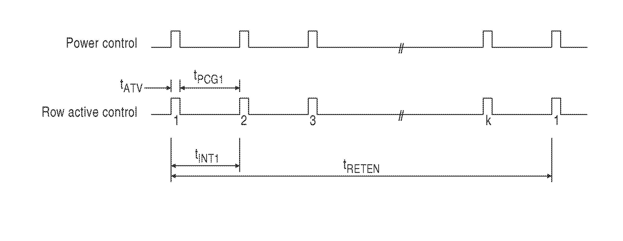
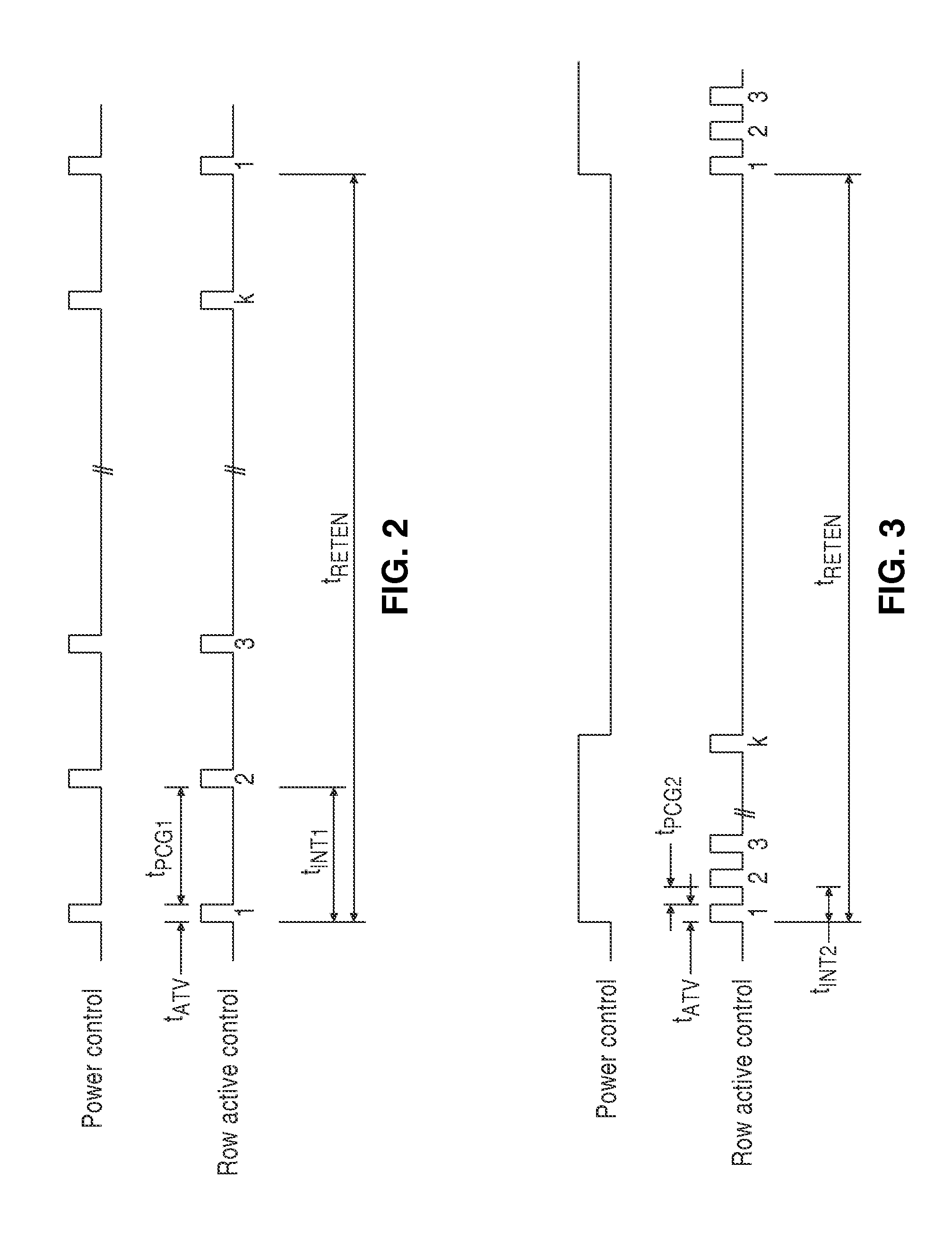
[0065] 1. Grouping of Refresh Cycles.

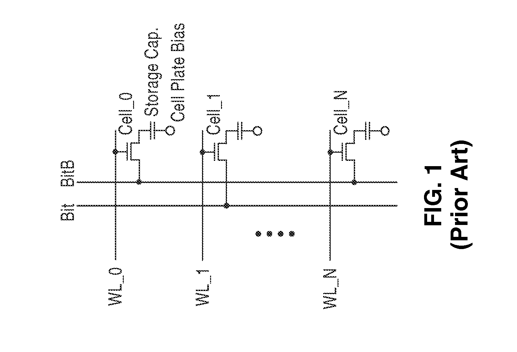
[0066] A DRAM cell, in absence of any intervention, loses its stored bit information as charge escapes through leakage paths. Therefore, data must be periodically rewritten to the cells in a refresh operation in order to maintain the stored information. In a refresh operation data is read from the cell and then the same data is rewritten into the cell thus recharging the charge storage element (e.g., capacitor), for example to an initial (full) level of charge for a “1” state, or fully depleting it for a “0” state. The present invention is more pa...


PUM


Abstract

Dynamic Random Access Memory (DRAM) circuits and methods are described for reducing leakage and increasing repaired yield. These objects are accomplished according to the invention by grouping refresh cycles within a single activation of power control, the use of limiting circuits or fuses to mitigate power losses associated with micro-bridging of bit-lines and word-lines, modulating the bit-line voltage at the end of precharge cycles, configuring refresh control circuits to use redundant word-lines in generating additional refresh cycles for redundant rows of memory cells, and combinations thereof. In one aspect, word-line fuses indicate modes of use as: unused, replacement, additional refresh, and replacement with additional refresh. The refresh control circuit utilizes these modes in combination with the X-address stored in the word-line fuses for controlling the generation of additional refresh cycles toward overcoming insufficient data retention intervals in select memory cell rows.

Description

CROSS-REFERENCE TO RELATED APPLICATIONS [0001] This application claims priority from U.S. provisional application Ser. No. 60 / 833,599, filed on Jul. 26, 2006, incorporated herein by reference in its entirety.STATEMENT REGARDING FEDERALLY SPONSORED RESEARCH OR DEVELOPMENT [0002] Not Applicable INCORPORATION-BY-REFERENCE OF MATERIAL SUBMITTED ON A COMPACT DISC [0003] Not Applicable NOTICE OF MATERIAL SUBJECT TO COPYRIGHT PROTECTION [0004] A portion of the material in this patent document is subject to copyright protection under the copyright laws of the United States and of other countries. The owner of the copyright rights has no objection to the facsimile reproduction by anyone of the patent document or the patent disclosure, as it appears in the United States Patent and Trademark Office publicly available file or records, but otherwise reserves all copyright rights whatsoever. The copyright owner does not hereby waive any of its rights to have this patent document maintained in sec...

Claims


Application Information

Patent Timeline
Patent Type & Authority Applications(United States)
IPC IPC(8): G11C7/00
CPCG11C11/406G11C11/4094G11C29/783G11C29/83G11C2211/4068G11C2211/4061G11C2211/4065G11C2211/4067G11C29/832
Inventor YOO, SEUNG-MOONCHOI, MYUNG CHANSHIN, SANGHOHAN, SANG-KYUN
Owner ZMOS TECH
Why Eureka
Try Eureka