Photoelectric conversion element and solid-state image pickup device

a technology of photoelectric conversion element and solid-state image pickup, which is applied in the direction of picture signal generator, television system, radioation control device, etc., can solve the problems of low sensitivities, inconvenient operation, and inability to accurately detect the color of the object, so as to achieve the effect of reducing the dark curren

Inactive Publication Date: 2008-02-14
FUJIFILM CORP
View PDF13 Cites 169 Cited by
  • Summary
  • Abstract
  • Description
  • Claims
  • Application Information

AI Technical Summary

Benefits of technology

[0021]The invention has been made on the basis of the considerations as mentioned above, and an object thereof is to provide a photoelectric conversion element which makes it possible...

Problems solved by technology

However, in the case of using color filters of primary colors, about two-thirds the incident light is absorbed by the color filters, so the single-plate solid-state color image pickup devices provided with such color filters arranged in mosaic patterns have a problem that they have low sensitivities because of inferior efficiencies in light utilization.
As a result thereof, the devices are inferior in resolution and have an additional problem that false colors in particular are conspicuous.
So it has been impossible to obtain elements with great photo current/dark current ratios.
In the structure shown in FIG. 18A, reduction in dark current is supposed to occur adequately since hole and electron blocking layers are provided, but the fact is that dark-current reduction worth expecting cannot be achieved.
However, when a voltage is applied externally to such an element, dark current is increased in actuality by carrier injection from the electrode via impurity levels and defect levels preset in the blocking layer, and to this problem the technique disclosed in JP-A-5-129576 offers no solution.
No matter what material is used, however, there occurs c...

Method used


Image

  • Photoelectric conversion element and solid-state image pickup device
  • Photoelectric conversion element and solid-state image pickup device
  • Photoelectric conversion element and solid-state image pickup device

Examples


first embodiment

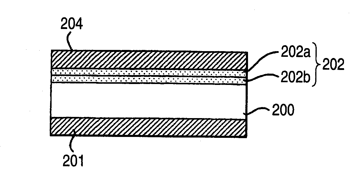
[0065]FIG. 1 is a schematic cross-sectional diagram showing an example of the structure of a photoelectric conversion element having a charge blocking layer according to an embodiment of the invention.

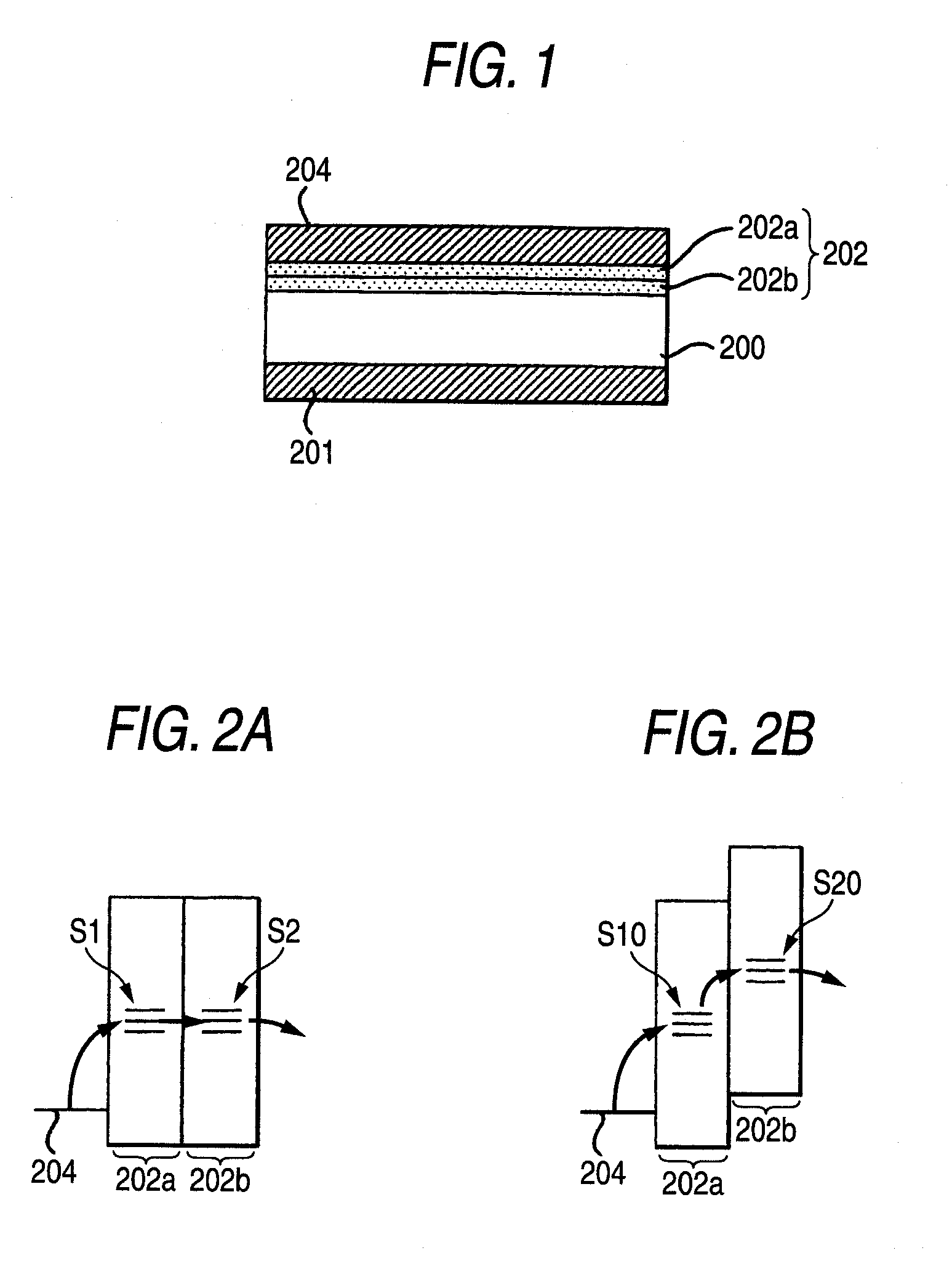
[0066]In FIG. 1, the reference numeral 200 represents a photoelectric conversion layer, the reference numeral 202 a charge blocking layer having a double-layer structure, the reference symbols 202a and 202b layers constituting the charge blocking layer 202, and the reference numerals 201 and 204 electrodes.

[0067]When the electrode 204 is arranged as, say, an electrode on the side of light incidence, it is necessary for the electrode 204 to transmit the incident light to the photoelectric conversion layer 200, so the electrode 204 is preferably made up of highly transparent materials. Examples of a highly transparent electrode include transparent conductive oxides (TCO). In addition, as seen in a configuration of the image pickup device illustrated hereinafter, there is a case where tra...

second embodiment

[0100]As to a second embodiment, examples of a photoelectric conversion element having a charge blocking layer of multiple-layer structure are illustrated by reference to FIG. 6 to FIG. 11.

[0101]There are two types of charge blocking layers—one being “a hole blocking layer” having a great barrier against hole injection from the adjacent electrode and high transport capacity of electrons as a photocurrent carrier, and one being “an electron blocking layer” having a great barrier against electron injection from the adjacent electrode and high transport capacity of holes as a photocurrent carrier. In organic luminescent elements, as disclosed in JP-A-11-339966 and JP-A-2002-329582, blocking layers using organic materials are already provided in order to prevent carriers from piercing through their respective luminescent layers. By inserting such an organic blocking layer between an electrode and a photoelectric conversion layer in a photoelectric conversion section, photoelectric conve...

third embodiment

[0140]Examples of the makeup of a solid-state image pickup device using the photoelectric conversion element having the structure shown in FIG. 11 are illustrated below. In the following description, FIG. 12 to FIG. 16 are referred to. In each of these figures also, both the hole blocking layer and the electron blocking layer have multiple-layer structures as in the foregoing embodiments. However, each blocking layer in FIG. 12 to FIG. 16 is not drawn in the form of multiple-layer division in particular for convenience in drawing diagrams.

[0141]FIG. 12 is a schematic cross-sectional diagram of a pixel of solid-state image pickup device, which illustrates a third embodiment of the invention. FIG. 13 is a schematic cross-sectional view of the intermediate layer shown in FIG. 12. This solid-state image pickup device includes a large number of pixels, each of which is the pixel shown in FIG. 12, disposed in array on one plane, and signals obtained from this one pixel can produce one pix...


PUM


Abstract

A photoelectric conversion element comprises a photoelectric conversion section that includes: a pair of electrodes; and a photoelectric conversion layer disposed between the pair of electrodes, wherein the photoelectric conversion section further comprises between one of the pair of electrodes and the photoelectric conversion layer a first charge-blocking layer that restrains injection of charges from the one of the electrodes into the photoelectric conversion layer when a voltage is applied to the pair of electrodes, and the first charge-blocking layer comprises a plurality of layers.

Description

BACKGROUND OF THE INVENTION[0001]1. Field of the Invention[0002]The present invention relates to a photoelectric conversion element, and more particularly to a photoelectric conversion element of the type which has a photoelectric conversion layer disposed between a pair of electrodes and undergoes application of a voltage to the pair of electrodes.[0003]2. Description of the Related Art[0004]In single-plate solid-state color image pickup devices, notably CCD and CMOS image sensors, three or four kinds of color filters are arranged in a mosaic pattern on a photoelectric conversion element array. By this arrangement, color signals corresponding to color filters are put out from individual photoelectric conversion elements, and these color signals are formed into color images through signal processing.[0005]However, in the case of using color filters of primary colors, about two-thirds the incident light is absorbed by the color filters, so the single-plate solid-state color image pic...

Claims


Application Information

Patent Timeline
IPC IPC(8): H01L31/00H01L27/146H01L31/10H04N5/335H04N5/361H04N5/369H04N9/07
CPCH01L27/14647H01L27/307H01L51/0059H01L51/0067H01L27/14605H01L51/0072H01L51/0081H01L51/4246Y02E10/549H01L51/0071C09B57/00C09B57/008H10K39/32H10K85/631H10K85/654H10K85/657H10K85/324H10K30/211H10K85/6572
Inventor HAYASHI, MASAYUKIMAEHARA, YOSHIKIMITSUI, TETSURO
Owner FUJIFILM CORP
Why Eureka
Try Eureka