
Integrated circuit wearout detection

a technology of integrated circuits and wearout detection, which is applied in the direction of electronic circuit testing, measurement devices, instruments, etc., can solve the problems of increasing power and current density, increasing the frequency of wearout-related failures in future technology generations, and unable to meet the reliability requirements of future technology. , to achieve the effect of increasing the operating voltage reducing the operating frequency of the integrated circuit, and increasing the power consumption

Inactive Publication Date: 2008-02-14
ARM LTD +1
View PDF12 Cites 51 Cited by
  • Summary
  • Abstract
  • Description
  • Claims
  • Application Information

AI Technical Summary

Benefits of technology

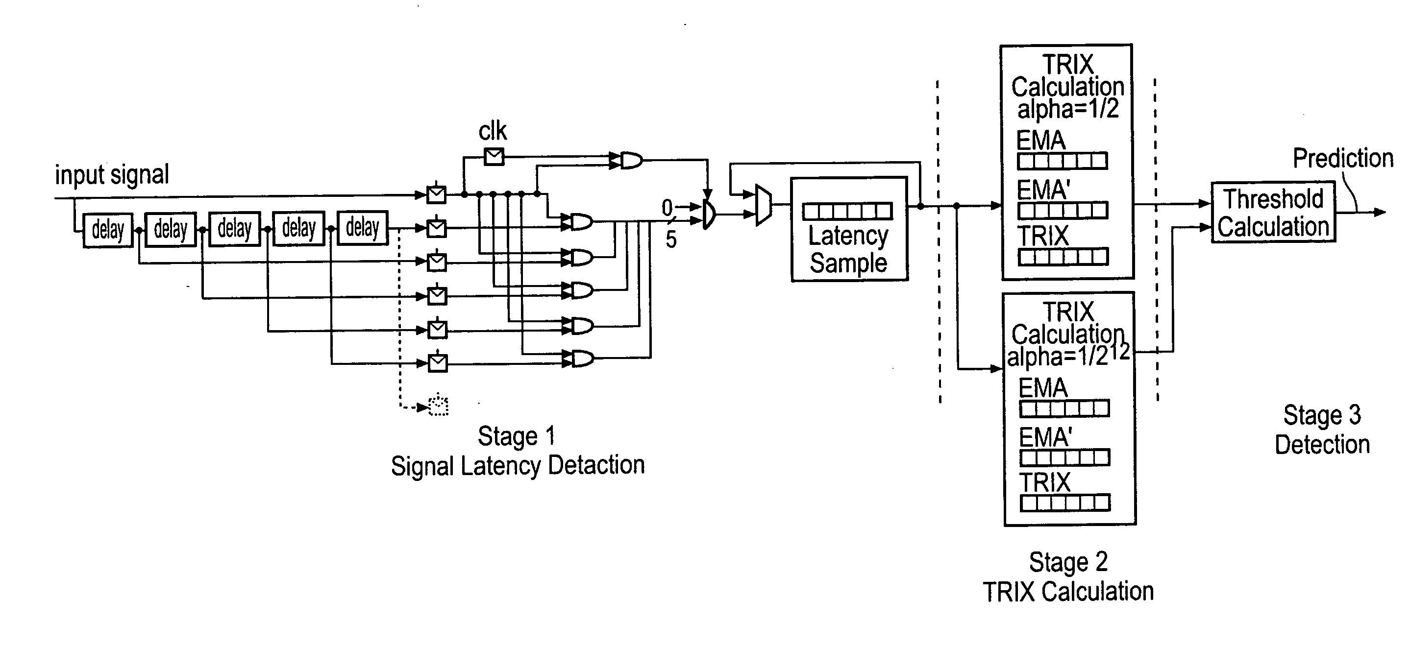
[0016]The wearout response which is triggered can take a wide variety of different forms. Cold swapping spare circuitry in place of circuitry in which imminent wearout failure has been detected is one example. Another example would be reducing the operating frequency of the integrated circuitry, such that it was operational but backed away from higher frequencies which could result in wearout failure due to excessive latency of certain signals.
[0022]The plurality of reference signals may be conveniently and accurately generated by a plurality taps from a delay line.

Problems solved by technology

However, projections of current technology trends indicate that these techniques will be unlikely to satisfy reliability requirements in future technology generations [11].
As CMOS feature sizes scale to smaller dimensions, voltage scales at a much slower rate, causing dramatic increases in power and current density.
Since the most common wearout mechanisms, such as electromigration (EM), time dependent dielectric breakdown (TDDB), hot carrier injection (HCI), and negative bias threshold inversion (NBTI) are all highly dependent on temperature, power, and current density, the occurrence of wearout-related failures will become increasingly common in future technology generations.
The use of redundant hardware is costly in terms of both power and area and does not significantly increase the lifetime of the processor without additional cold-spare devices, which further increases the cost of such techniques.
Redundancy in time is potentially less expensive, but may only provide transient error detection without correction unless redundant hardware is readily available.
Failure prediction techniques are typically less costly to implement, however, they also face a number of challenges.
Canary circuits are an efficient and generic means to predict failure, however there are a number of sensitive issues that must be addressed to deploy them effectively.

Method used


Image

  • Integrated circuit wearout detection
  • Integrated circuit wearout detection
  • Integrated circuit wearout detection

Examples


Embodiment Construction

Background

[0045]In order to better understand the physical phenomenon that cause wearout and why technology scaling has such a dramatic impact on lifetime reliability, we briefly discuss a subset of the wearout mechanisms that plague modern integrated circuit designs (e.g. microprocessor designs). This section presents industry-standard theoretical models for each wearout mechanism and discusses how these mechanisms affect circuit-level timing within the design.

Electromigration (EM)

[0046]EM is a physical phenomenon that causes the mass transport of metal within semiconductor interconnects. As electrons flow through the interconnect, momentum is exchanged when they collide with metal ions. This pushes metal ions in the direction of electron flow and, at high current densities, results in the formation of voids (regions of metal depletion) and hillocks (regions of metal deposition) in the conductor metal [13].

[0047]The model of electromigration that we employ is based on a version of ...


PUM


Abstract

An integrated circuit is provided with latency detecting circuitry for detecting signal generation latency within one or more functional circuits and in response thereto to generate a wearout response. The wearout response can take a variety of different forms such as reducing the operating frequency, increasing the operating voltage, operating task allocation within a multiprocessor system, manufacturing test binning and other wearout responses.

Description

BACKGROUND OF THE INVENTION[0001]1. Field of the Invention[0002]This invention relates to the field of integrated circuits. More particularly, this invention relates to the detection of wearout due to operation of integrated circuits.[0003]2. Description of the Prior Art[0004]Traditionally, microprocessors have been designed with the worst case operating conditions in mind. To this end, manufactures have employed burn in, guard bands, and speed binning to ensure that processors will meet a predefined lifetime qualification, or mean time to failure (MTTF). However, projections of current technology trends indicate that these techniques will be unlikely to satisfy reliability requirements in future technology generations [11]. As CMOS feature sizes scale to smaller dimensions, voltage scales at a much slower rate, causing dramatic increases in power and current density. Areas of high power density increase local temperatures leading to hot spots on the chip [27]. Since the most common...

Claims


Application Information

Patent Timeline
IPC IPC(8): G01R31/26
CPCG01R31/31708G01R31/287
Inventor BRADLEY, DARYL WAYNEBLOME, JASON ANDREWMAHLKE, SCOTT
Owner ARM LTD
Learn More