

Snubber Circuit and Power Semiconductor Device Having Snubber Circuit
a technology of snubber circuit and power semiconductor device, which is applied in the direction of circuit arrangement, emergency protective arrangement for limiting excess voltage/current, dc-ac conversion without reversal, etc., can solve the problems of a relatively large number of component parts, increase the size of the inverter device, and reduce space efficiency. , to achieve the effect of increasing the reliability of the power semiconductor device, reducing the area of the chip, and reducing the electrostatic capacity
- Summary
- Abstract
- Description
- Claims
- Application Information
AI Technical Summary
Benefits of technology
Problems solved by technology
Method used
Image

Examples
first embodiment
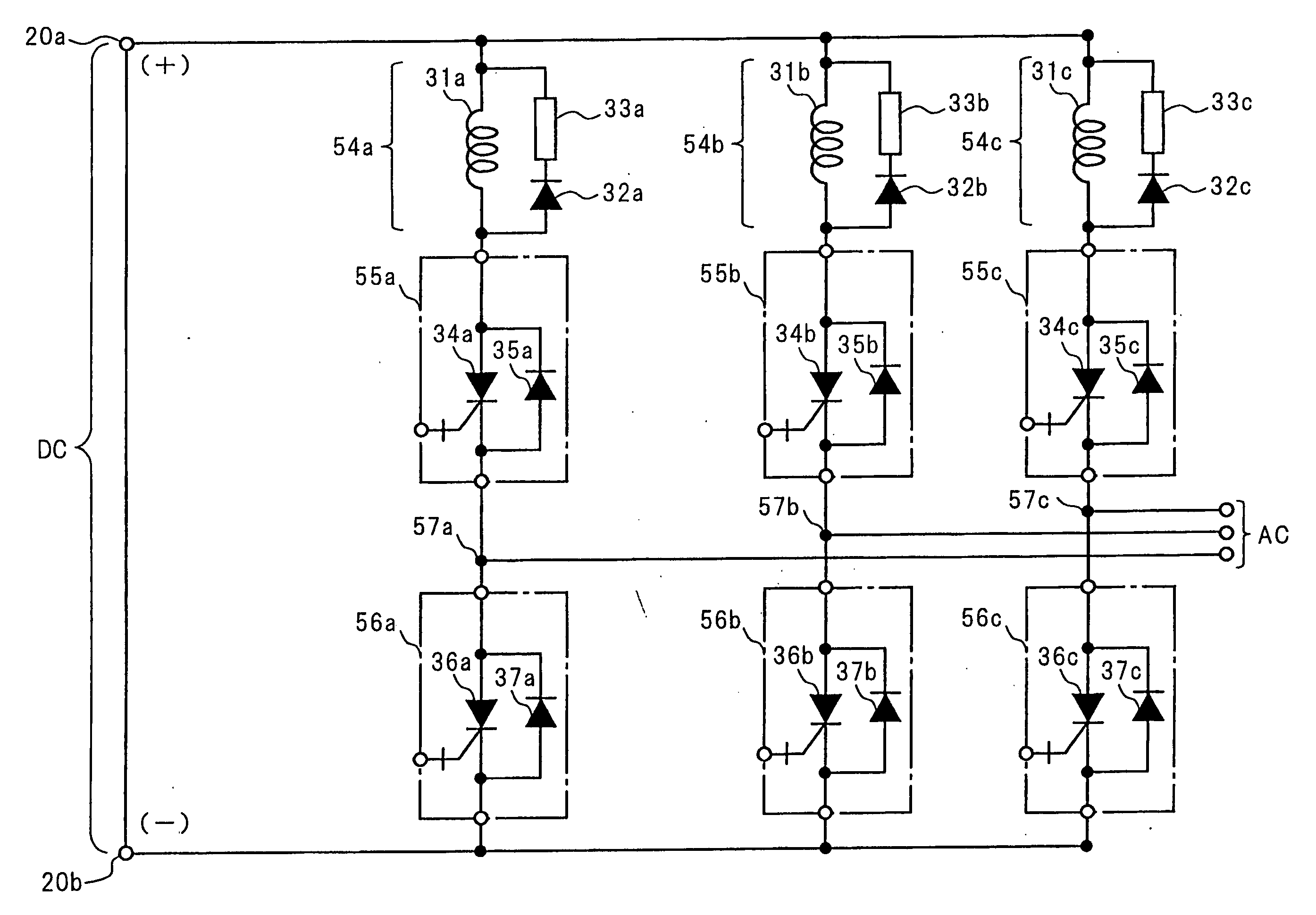
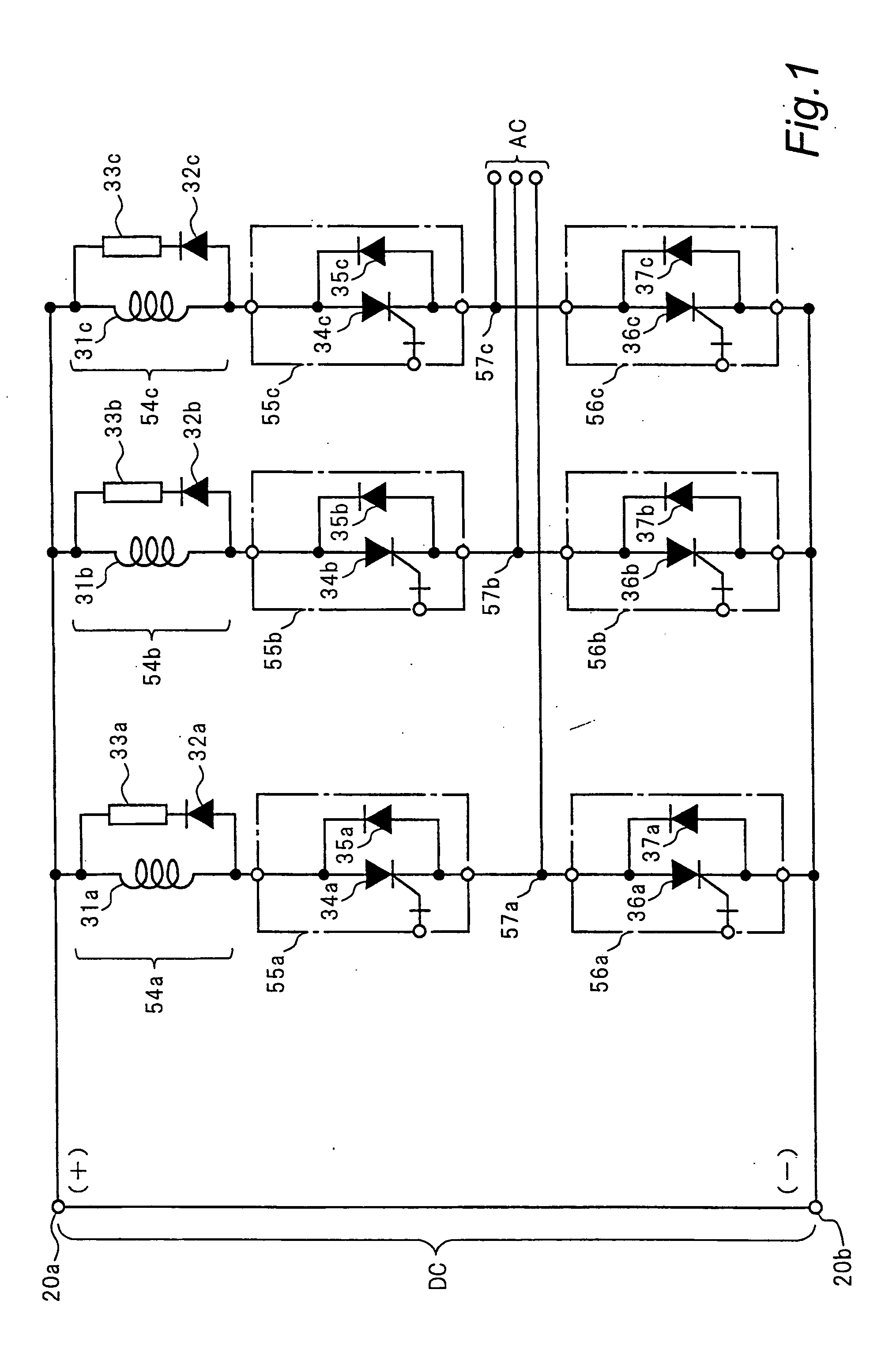
[0060] A three-phase inverter device, that is a power semiconductor device in the first embodiment of the present invention, will be described with reference to FIG. 1. In the drawing, a series connection formed by connecting a series snubber circuit 54a, a first switching circuit 55a and a second switching circuit 56a in this order is connected to between a positive terminal 20a and a negative terminal 20b of a direct current input DC (direct current power supply). Similarly, a series connection composed of a series snubber circuit 54b, a first switching circuit 55b and a second switching circuit 56b is connected to between the positive terminal 20a and the negative terminal 20b. A series connection composed of a series snubber circuit 54c, a first switching circuit 55c and a second switching circuit 56c is connected to between the positive terminal 20a and the negative terminal 20b. The series snubber circuit 54a, and the first and second switching circuits 55a, 56a should not nec...
second embodiment
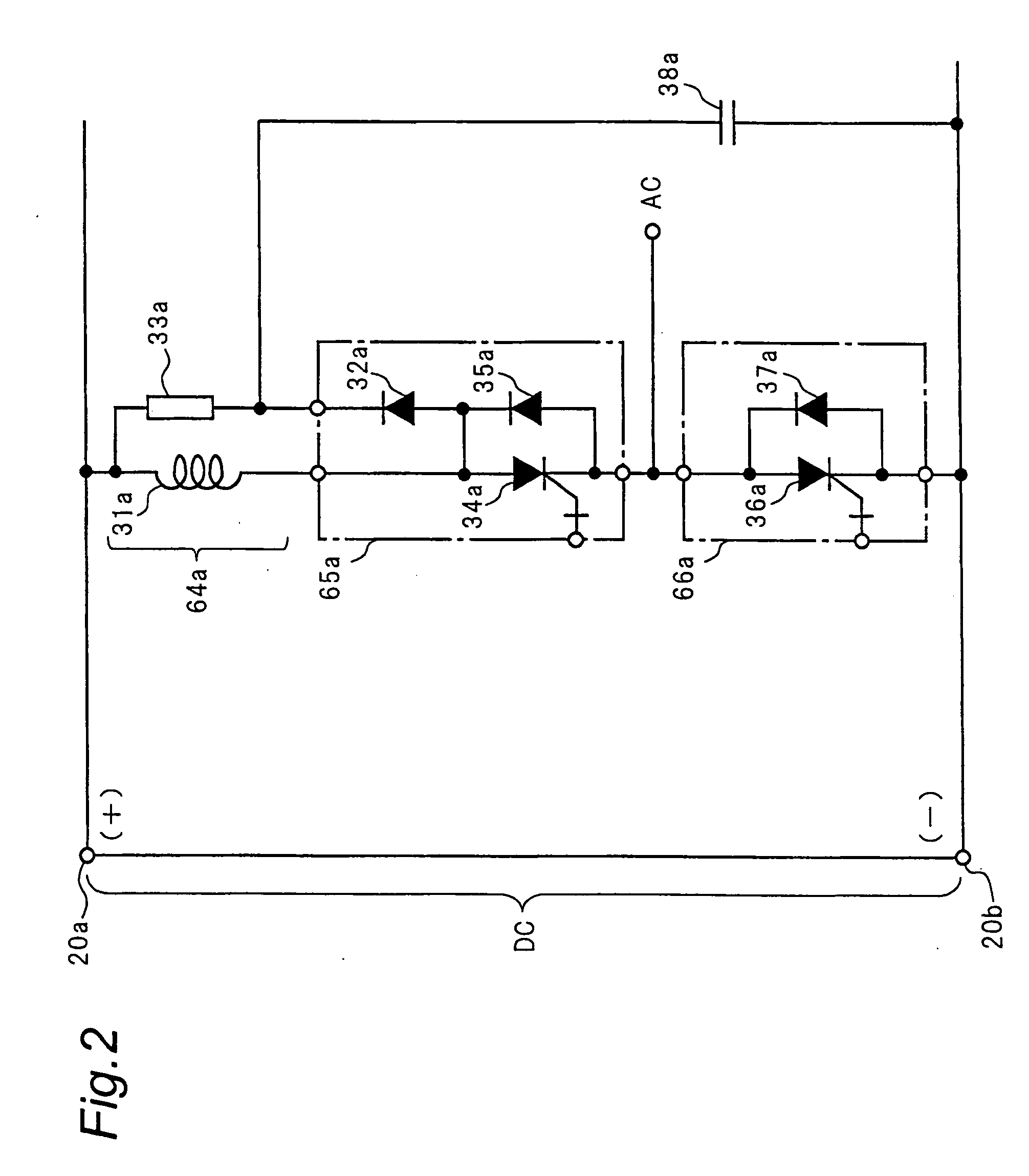
[0077] Description is now given of a three-phase inverter device that is a power semiconductor device in a second embodiment of the present invention with reference to FIG. 2. FIG. 2 is a circuit diagram showing a switching circuit of one phase in the three-phase inverter device in the second embodiment of the present invention. In the drawing, a series connection composed of a snubber circuit 64a, a first switching circuit 65a and a second switching circuit 66a is connected to between a positive terminal 20a and a negative terminal 20b of a direct input DC (direct current power supply). While the actual three-phase inverter device is composed of three series connections of three phases which share the same structure and the same operation and which are connected to between the positive terminal 20a and the negative terminal 20b, only one phase is shown in the drawing and illustration and description of other two phases are omitted for simplification. While the three-phase inverter ...
third embodiment
[0085] Description is now given of a three-phase inverter device that is a power semiconductor device in a third embodiment of the present invention with reference to FIG. 3. FIG. 3 is a circuit diagram showing a switching circuit of one phase in the three-phase inverter device, and the circuits of other two phases are omitted. In FIG. 3, a series snubber circuit 64a composed of an anode reactor 31a, a SiC diode 32a and a resistance 33a is similar to that in the second embodiment shown in FIG. 2.
[0086] A first switching circuit 65a has a SiC-GTO 34a and a SiC free wheeling diode 35a connected in antiparallel, and the SiC-GTO 34a and the SiC diodes 32a, 35a are incorporated in a single package. A clamp capacitor 38a is connected to between the cathode of the SiC diode 32a and the negative terminal 20b, while a snubber capacitor 40a is connected to between the cathode of the SiC diode 32a and the cathode of the SiC-GTO 34a. The SiC diode 32a and the snubber capacitor 40a constitute a...
PUM
 Abstract
Description
Claims
Application Information