System and method of maximizing integrated circuit manufacturing yield with fabrication process simulation driven layout optimization

a technology of layout optimization and fabrication process, applied in the direction of cad circuit design, program control, instruments, etc., can solve the problems of high overall cost of good ics, poor fabricated ics, and insufficient accuracy of semiconductor structures to ensure correct circuit operation. , to achieve the effect of maximizing manufacturing yield

Inactive Publication Date: 2008-02-21
CHEW MARKO P +1
View PDF1 Cites 326 Cited by
  • Summary
  • Abstract
  • Description
  • Claims
  • Application Information

AI Technical Summary

Benefits of technology

[0029]These and other objects, features and advantages in accordance with the present invention are provided by a sy

Problems solved by technology

The IC fabrication process is such an extremely complex process so that the sequence of IC fabrication process steps indicated by an IC mask data might not produce the semiconductor structures with sufficient accuracy to assure correct circuit operation.
If there are too many discard ICs, then the yield or fraction of good IC will be low and results in higher overall cost for the good ICs.
Any issue with the various steps in IC fabrication procedure could cause the resulting semiconductor structures to deviate sufficiently to cause the fabricated IC to be bad.
Starting at the 130 nm process node and continuing to the current process nodes, the interaction of process and design has made this task much more difficult.
This is because it is no longer possible to have a fabrication process recipe that produces the optimal yield for all possible mask layout data.
Any loss of fidelity on the transferred pattern from that of the mask may result in decreased in IC yield.
However, since it does not consider design context of layout geometries, its functionality and effectiveness is very much limited.
OPC verification tools may find OPC violations that happen due to reasons such as, but not limited to, design patterns beyond usage under which OPC recipes are developed; limitation of OPC recipes on various process corners; and certain design patterns are inherently difficult to be adjusted for OPC.
While it is possible to fix OPC violations that are due to limited OPC recipes or incomplete design pattern coverage of OPC recipes through use

Method used


Image

  • System and method of maximizing integrated circuit manufacturing yield with fabrication process simulation driven layout optimization
  • System and method of maximizing integrated circuit manufacturing yield with fabrication process simulation driven layout optimization
  • System and method of maximizing integrated circuit manufacturing yield with fabrication process simulation driven layout optimization

Examples


Embodiment Construction

[0041]EMBODIMENTS

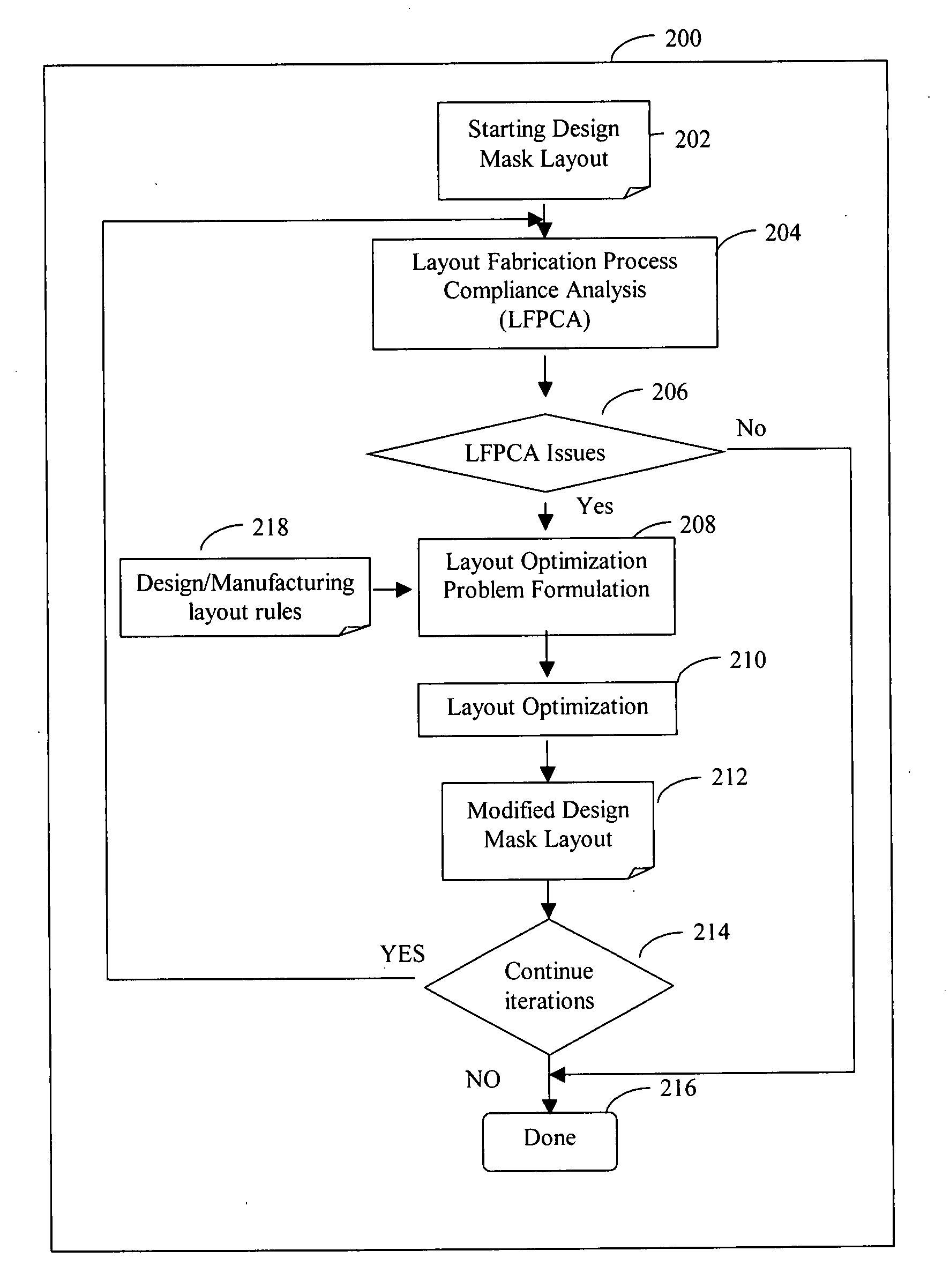
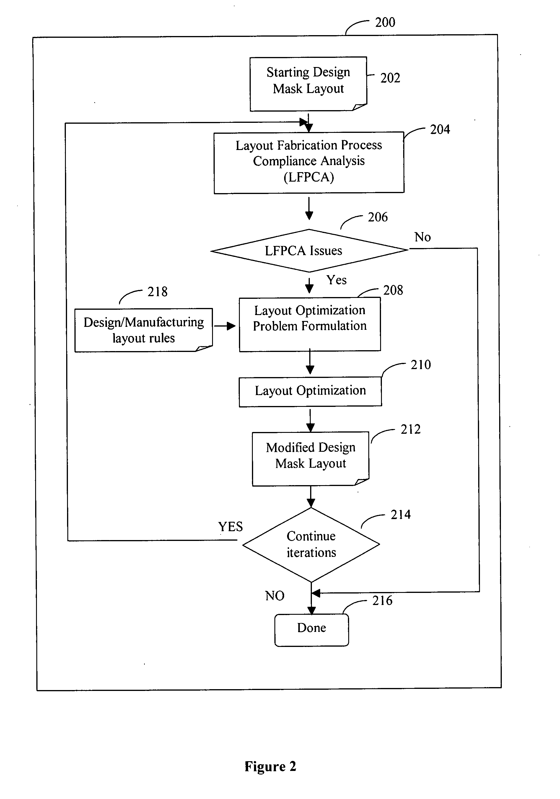
[0042]This invention relates to an integrated circuit mask layout optimization system and an integrated circuit mask layout optimization method, and more to a methodology for maximizing manufacturing yield by using automatic layout optimization driven by IC fabrication process simulation and layout fabrication process compliance analysis. The present invention describes a system and a method of representing layout using a set of variables; formulating metrics of fabrication process quality which is directly correlated to manufacturing yield through LFPCA; identifying a function of sensitivity of each variable representing design to the metrics of LFPCA quality and formulating an optimization problem to maximize manufacturing yield by changing the variables representing a design mask layout data within predefined ranges and within the constraints imposed by design rules and other requirements; iterating the procedure in order to converge to a final optimized result.

[...


PUM


Abstract

A system and a method of maximizing the manufacturing yield of integrated circuit (“IC”) design using IC fabrication process simulation driven layout optimization is described. An IC design layout is automatically modified through formulation of a layout optimization problem utilizing the results of layout fabrication process compliance analysis tools. The modification of layout is performed adaptively and iteratively to make an IC layout less susceptible to yield issues while maintaining design rule correctness and minimal circuit performance impact.

Description

CLAIM OF BENEFIT TO PROVISIONAL APPLICATION[0001]This patent application claims the benefit of the earlier filed U.S. Provisional Patent Application entitled “System and method of maximizing integrated circuit manufacturing yield with fabrication process simulation driven layout optimization”, having Ser. No. 60 / 838,023, and filed Aug. 15, 2006.TECHNICAL FIELD OF APPLICATION[0002]This invention relates generally to the design and manufacture of integrated circuitry and more particularly to a system and a method of maximizing manufacturing yield by using layout optimization driven by integrated circuit fabrication process simulation.BACKGROUND OF THE INVENTION[0003]The electronic circuit of an integrated circuit (“IC”) consists of connected components such as transistors, diodes and resistors. The description of the components and their interconnections is called a netlist. Each component is mapped to one or more layout objects that are two-dimensional geometrical objects such as, bu...

Claims


Application Information

Patent Timeline
IPC IPC(8): G06F17/50
CPCG06F17/5068G06F30/39
Inventor CHEW, MARKO P.YANG, YUE
Owner CHEW MARKO P
Why Eureka
Try Eureka