

Apparatus and method for treating substrates
- Summary
- Abstract
- Description
- Claims
- Application Information
AI Technical Summary
Benefits of technology
Problems solved by technology
Method used
Image

Examples
first embodiment
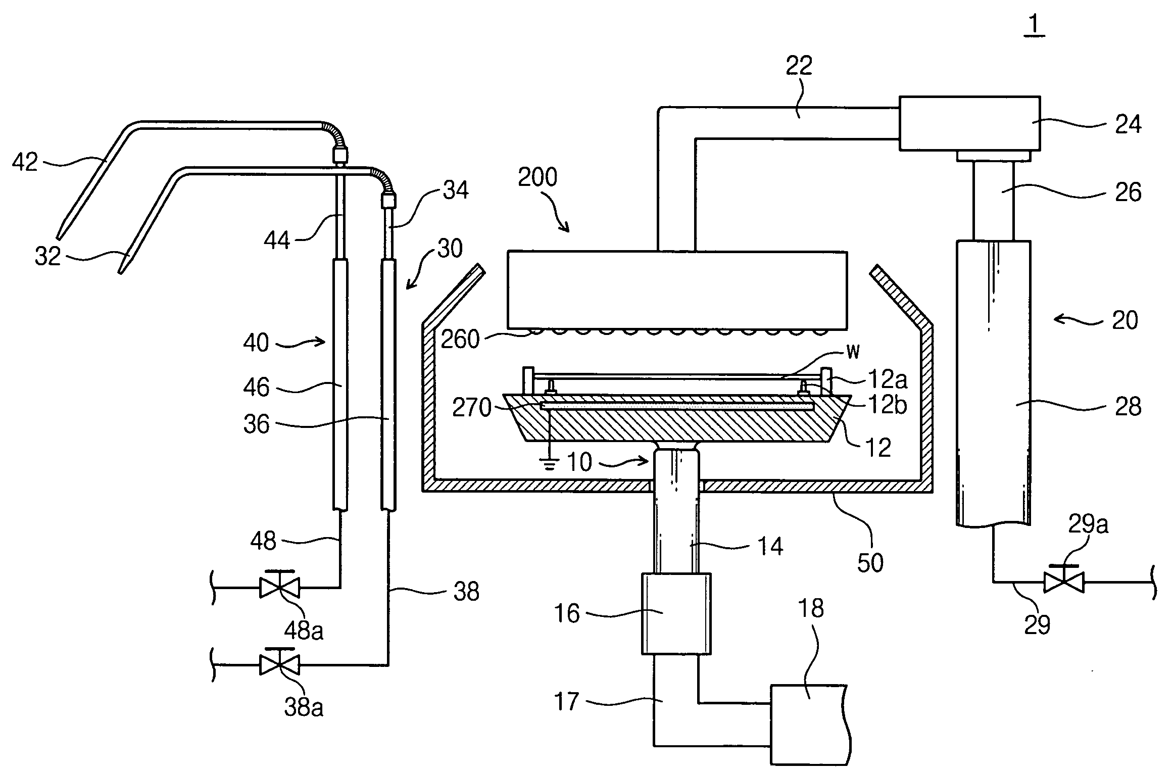
[0023]FIG. 1 illustrates a substrate treating apparatus 1 according to the present invention. The substrate treating apparatus 1 includes a support part 10, a dry-type treating part 20, a wet-type treating part 30, a drying part 40, and a container 50.
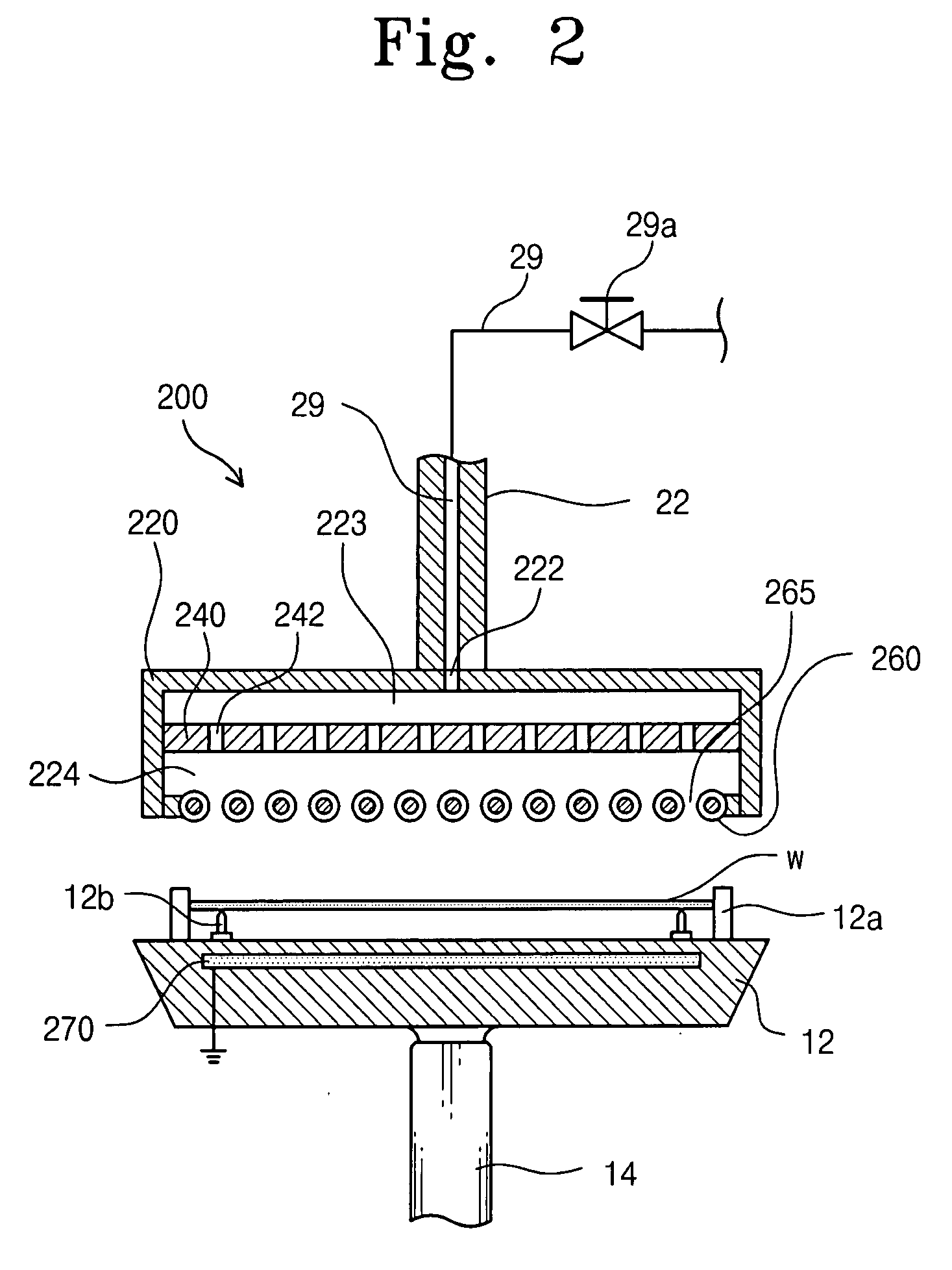
[0024]The support part 10 is configured to support a wafer W such that a pattern surface of the wafer W faces upwardly. The support part 10 includes a plate 12 and a support shaft 14 connected to the bottom of the plate 12.
[0025]The plate 12 roughly exhibits the shape of a disk. A wafer W is loaded on the plate 12 to be stacked abreast. A plurality of chucking pins 12a and a plurality of support pins 12b are provided on the top surface of the plate 12. The chucking pins 12a are disposed at the edge of the plate 12 to support a side portion of the loaded wafer W, and the support pins 12b are disposed inside the chucking pins 12a to support the bottom of the loaded wafer W.
[0026]The support shaft 14 is connected to the bottom of the plat...
second embodiment
[0080]FIG. 8 illustrates a flowchart illustrating a substrate treating method according to the present invention. Steps S110-S140 of FIG. 8 are identical to those described with reference to FIG. 7.
[0081]The wafer W is cleaned by means of a wet-type treating part 30 (S150). The wet-type treating part 30 supplies a cleaning solution onto the wafer W. When a valve 38a is opened, the cleaning solution is supplied to a chemical nozzle 32 along a chemical line 38. The supplied cleaning solution is injected onto the rotating wafer W through the chemical nozzle 32.
[0082]The cleaning solution is the standard clean-1 (SC-1), which is the mixture of ammonium hydroxide (NH4OH), hydrogen peroxide (H2O2), and water (H2O) with a mixture of approximately 1:1:5˜0.05:1:5 at a temperature ranging from 80 to 90 degrees centigrade. The SC-1 is used to remove particles and organic contaminants. However, another cleaning solution may be used.
[0083]While “a cleaning solution is supplied along a chemical l...
third embodiment
[0086]FIG. 9 is a flowchart illustrating a substrate treating method according to the present invention. Steps S210-S260 of FIG. 9 are identical to the steps S110-S160 described with reference to FIG. 8.
[0087]An oxide layer on a wafer W is etched by means of a wet treatment part 30 (S270). The wet-type treating part 30 supplies an etching solution onto a wafer W. When a valve 38a is opened, the etching solution is supplied to a chemical nozzle 32 along a chemical line 38. The supplied etching solution is injected onto the rotating wafer W through the chemical nozzle 32.
[0088]The etching solution is hydrofluoric acid diluted using deionized water (deionized H2O). The diluted hydrofluoric acid (DHF) is used to effectively remove chemical oxide or native oxide generated during various cleaning processes. Moreover, the DHF may be used to effectively remove metal contaminants contained in oxide. However, another etching solution may be used.
[0089]While “an etching solution is supplied al...
PUM
| Property | Measurement | Unit |
|---|---|---|
| Power | aaaaa | aaaaa |
| Diameter | aaaaa | aaaaa |
| Length | aaaaa | aaaaa |
Abstract
Description
Claims
Application Information