

Organic Field-Effect Transistor and Semiconductor Device Including the Same
- Summary
- Abstract
- Description
- Claims
- Application Information
AI Technical Summary
Benefits of technology
Problems solved by technology
Method used
Image

Examples
embodiment mode 1
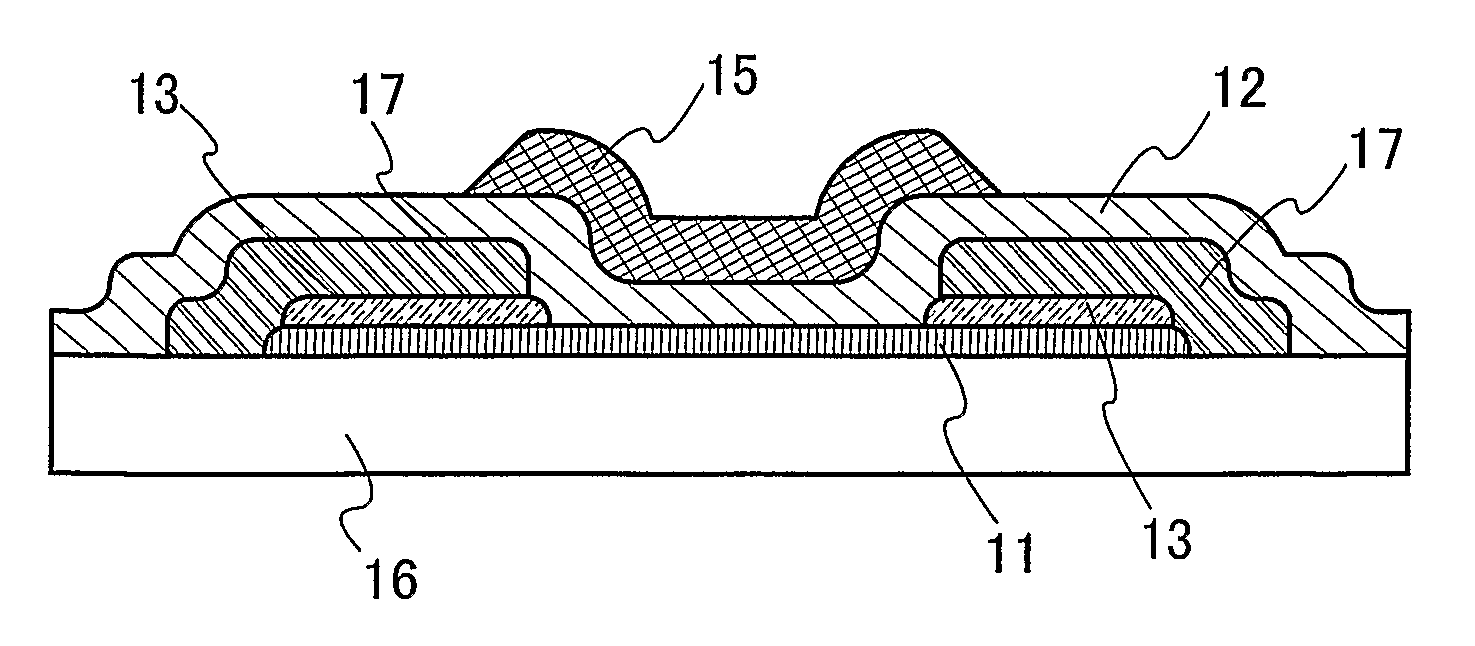
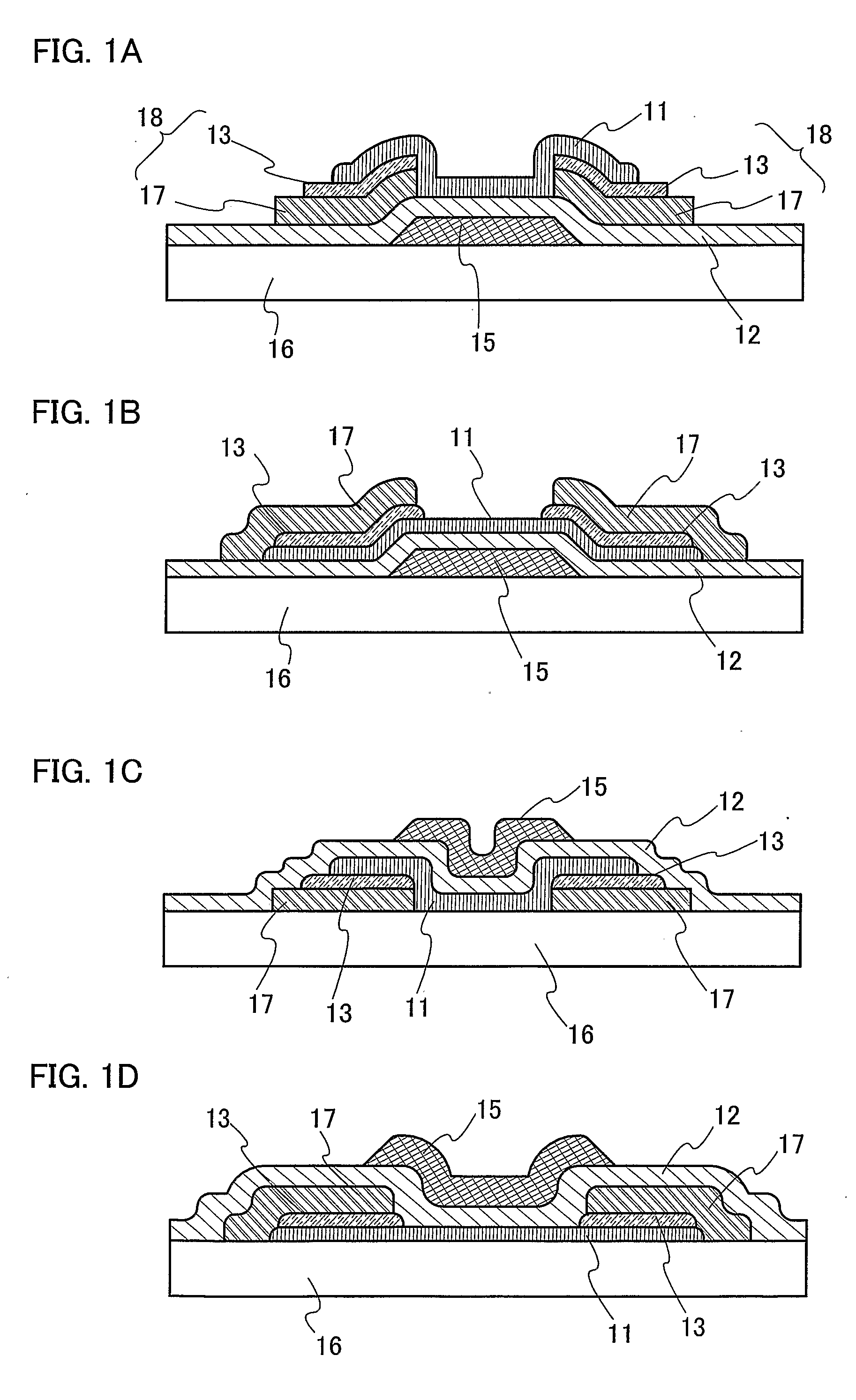
[0049] A constructional example of an organic field-effect transistor of the present invention will be described with reference to FIGS. 1A to 1D. Note that reference numeral 11 denotes a semiconductor layer including an organic semiconductor material; 12, an insulating layer; 13, a composite layer; 15, a gate electrode; and 16, a substrate. Each of source and drain electrodes 18 includes the composite layer 13 and a conductive layer 17. The alignment of each layer and each electrode can be appropriately selected in accordance with an application of an element. In the drawings, the composite layer 13 is provided to be in contact with the semiconductor layer 11, however the present invention is not limited to this, and the composite layer 13 may be included in a part of the source electrode and / or the drain electrode. The alignment of each layer and the electrode can be appropriately selected from FIGS. 1A to 1D in accordance with an application of an element.
[0050] As the substrate...
embodiment mode 2
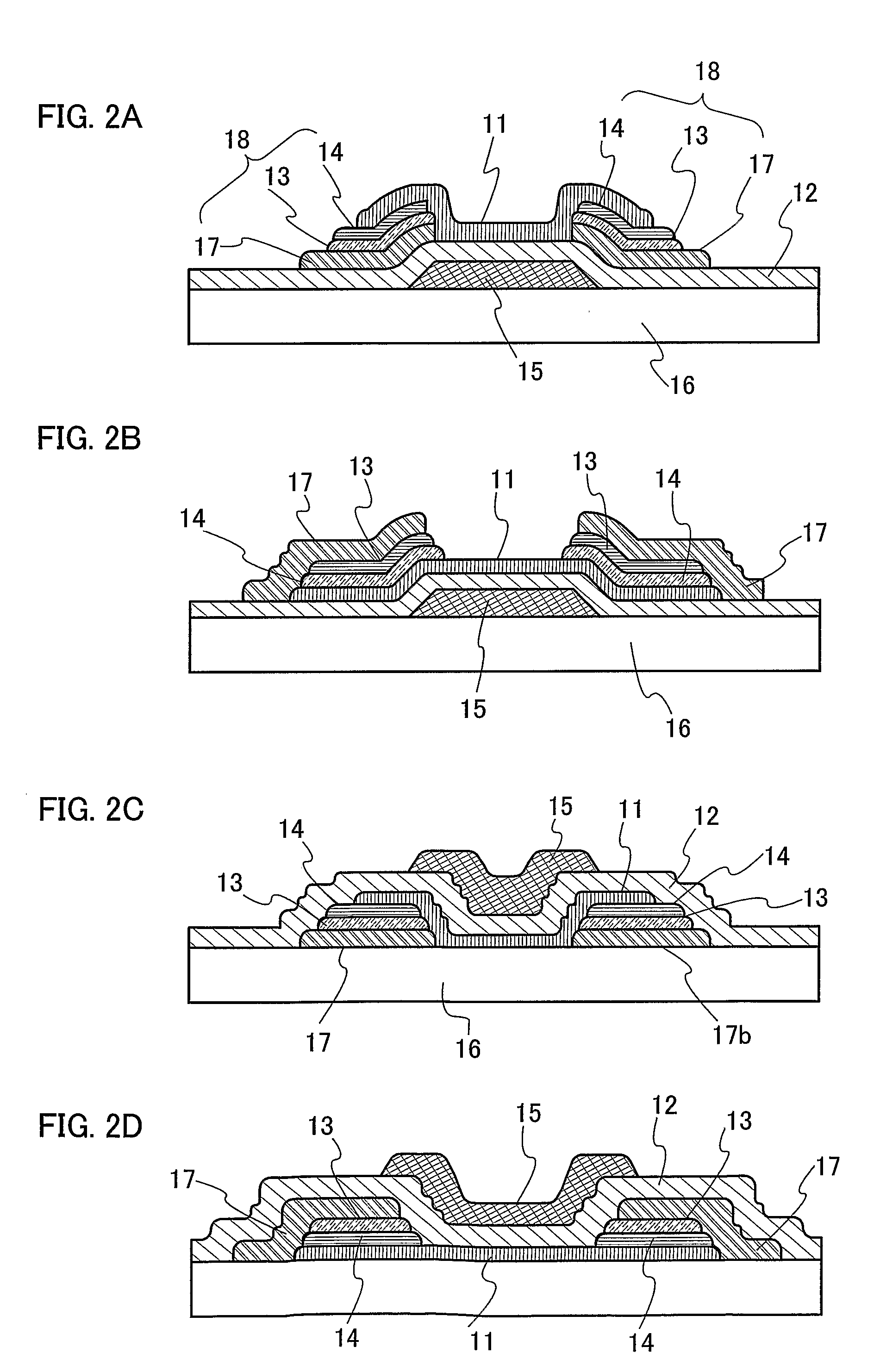
[0068] Next, a structure which is suitable for an n-type organic field-effect transistor having an electron as a carrier will be described as an example. This structure has a second layer 14 further including an alkali metal, an alkaline earth metal, or a compound (oxide, nitride or salt) including them, in addition to the structure of Embodiment Mode 1 having the composite layer 13 in a part of the source and drain electrodes.
[0069] An organic semiconductor material used in the present invention is not especially limited. However, specifically as the organic semiconductor material showing the characteristic as an n-channel field-effect transistor, perylenetetracarboxylic acid anhydride and derivatives thereof; perylenetetracarboxydiimie derivatives; naphthalenetetracarboxylic acid anhydride and derivatives thereof; naphthalenetetracarboxydiimide derivatives; metallophthalocyanine derivatives; fullerene; and the like, are preferable.
[0070] A kind of an alkali metal and an alkaline...
embodiment mode 3
[0079] Subsequently, a structure in which the organic compound used for the composite layer is also used for the semiconductor layer, will be described. In this structure, the organic compounds used for the composite layer and the semiconductor layer are the same, and therefore a manufacturing process becomes simple and costs can be reduced, which are the advantages. Furthermore, the adhesiveness between the semiconductor layer and the source electrode and between the semiconductor layer and the drain electrode, and the chemical stability of the interface therebetween are increased, and therefore further improvement of the transistor characteristic is expected. Also, the improvement of the durability of the organic field-effect transistor is expected.
[0080] A semiconductor material used in the present invention is not especially limited, however an aromatic amine compound is preferable since the material same as the organic compound used for the composite layer, is used.
[0081] The...
PUM
 Abstract
Description
Claims
Application Information