

Nonvolatile memory
- Summary
- Abstract
- Description
- Claims
- Application Information
AI Technical Summary
Benefits of technology
Problems solved by technology
Method used
Image

Examples
embodiment mode 1
[0035]This embodiment mode describes a circuit diagram, a driving method, and a cross-sectional structure of a memory cell, of a nonvolatile memory of the present invention.
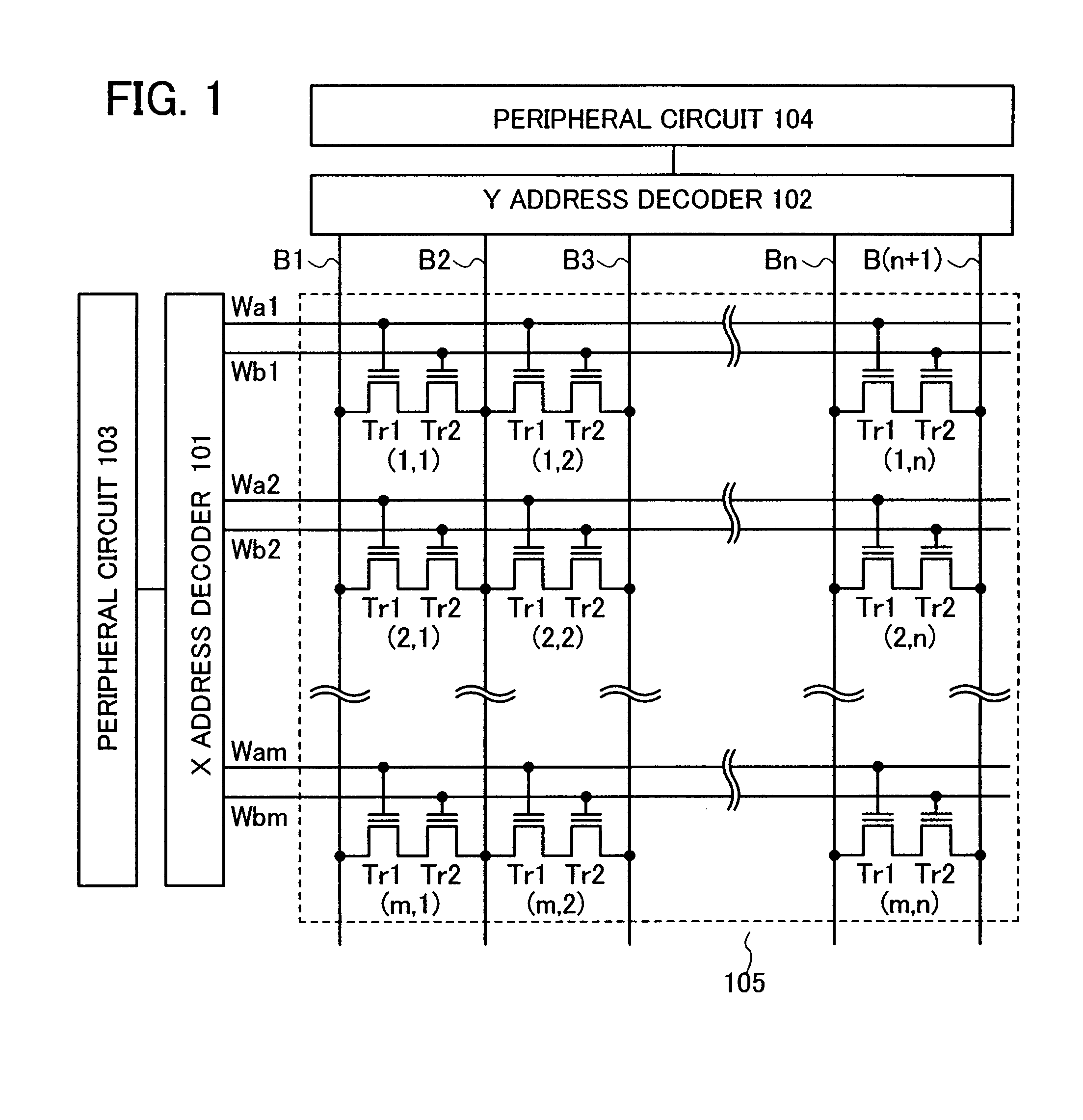
[0036]FIG. 1 shows circuits of a nonvolatile memory described in this embodiment mode. Shown as an example here is a circuit diagram of a (m×n)-bit nonvolatile memory (m and n are integers which are greater than or equal to 1).
[0037]The nonvolatile memory described in this embodiment mode includes a memory cell array 105 in which (m×n) memory cells (1, 1) to (m, n) are arranged in matrix so as to be m memory cells in row and n memory cells in column, an X address decoder 101 and a Y address decoder 102 which are driver circuits of the memory cell array 105, and other peripheral circuits 103 and 104.
[0038]Each memory cell (typically, a memory cell (i, j) is considered) (i is an integer which is greater than or equal to 1 and less than or equal to m, and j is an integer which is greater than or equal to 1 and less ...
embodiment mode 2
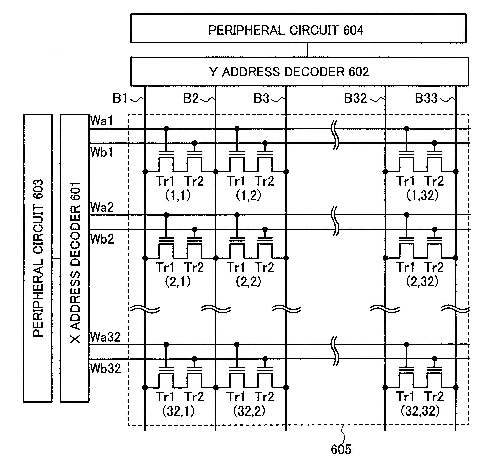
[0084]This embodiment mode describes a 2048-bit nonvolatile memory which includes p-channel transistors is described as an example of the nonvolatile memory of the present invention with reference to the drawing.
[0085]FIG. 11 is a circuit diagram of the nonvolatile memory of this embodiment mode. The nonvolatile memory shown in FIG. 11 includes a memory cell array 605 in which 1,024 memory cells (1, 1) to (32, 32) are arranged in matrix so as to be 32 memory cells in column and 32 memory cells in row, an X address decoder 601, a Y address decoder 602, and other peripheral circuits 603 and 604. Each memory cell includes two p-channel transistors Tr1 and Tr2. In the case where 1-bit data is stored in each memory transistor, the nonvolatile memory of this embodiment mode has a storage capacity of 2048 bits. The above-described other peripheral circuits include an address buffer circuit, a control logic circuit, a sense amplifier, a voltage step-up circuit, and the like, which are provi...
embodiment mode 3
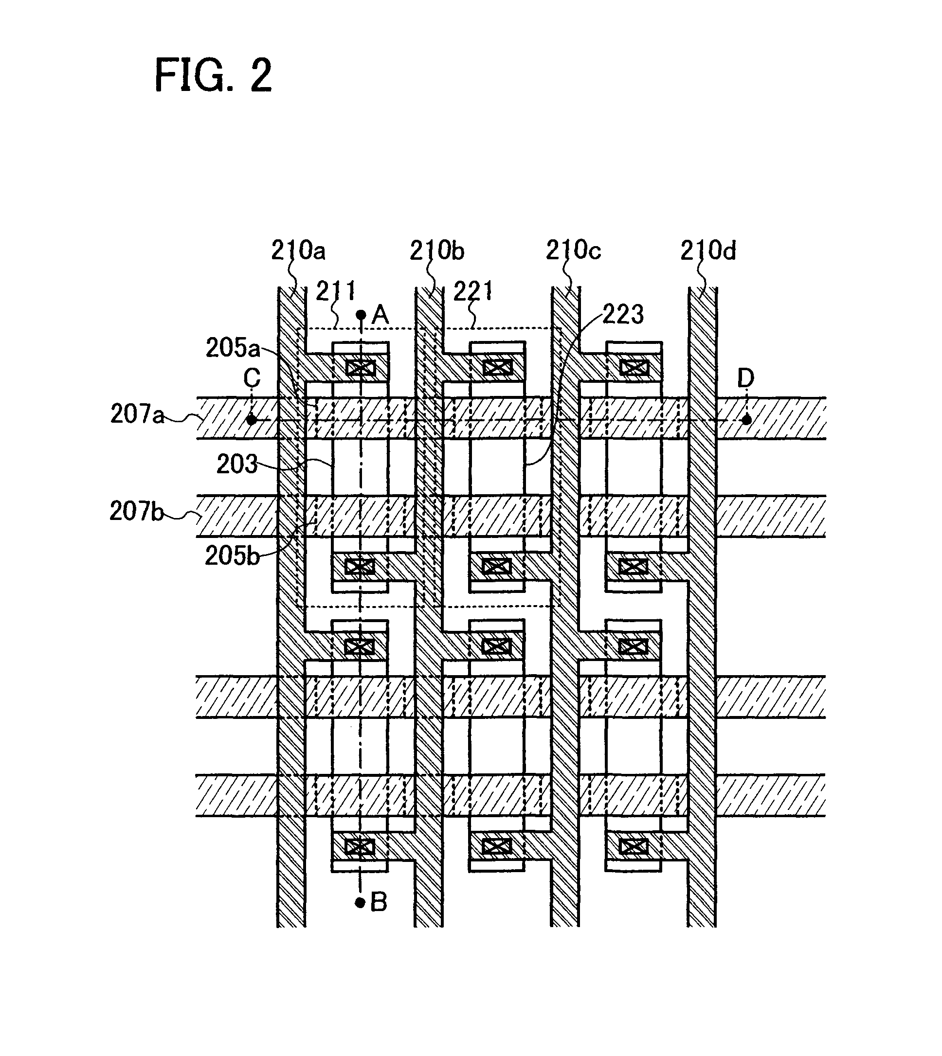
[0096]This embodiment mode describes one example of a manufacturing method of the nonvolatile memory of the present invention with reference to the drawings. Note that in the description below, as elements included in the nonvolatile memory, two memory transistors (n-channel memory TFTs) provided in a memory cell and two thin film transistors (a p-channel TFT and an n-channel TFT) included in a CMOS circuit which is a driver circuit of the memory cells or another peripheral circuit are described.
[0097]First, island-shaped semiconductor films 808, 810, and 812 are formed over a substrate 802 with an insulating film 804 interposed therebetween (FIG. 7A). The island-shaped semiconductor films 808, 810, and 812 can be provided as follows: an amorphous semiconductor film is formed of a material containing silicon (Si) as its main component (e.g., SixGe1-x) by a sputtering method, an LPCVD method, a plasma CVD method, or the like over the insulating film 804 formed in advance over the sub...
PUM
 Abstract
Description
Claims
Application Information