Transparent conductive film and method for manufacturing the same
a technology of transparent conductive film and manufacturing method, which is applied in the direction of oxide conductors, conductive layers on insulating supports, non-metal conductors, etc., can solve the problems of increasing the requirement of high cost of indium, and increasing the need for electrodes using other materials, etc., and achieve excellent economic effects
- Summary
- Abstract
- Description
- Claims
- Application Information
AI Technical Summary
Benefits of technology
Problems solved by technology
Method used
Image
Examples
example 1
[0115]A glass substrate composed of non-alkali glass (Corning 7059) was prepared as a substrate, and the glass substrate was washed with isopropyl alcohol and UV irradiation to form a clean surface.
[0116]Also, as a sputtering target, a ZnO sintered target having a sintering density of 80% or more and a diameter of 6 inches was prepared.
[0117]Furthermore, pellets (Ga2O3 pellets) of 10 mm in diameter and composed of Ga oxide (Ga2O3) were prepared for doping.
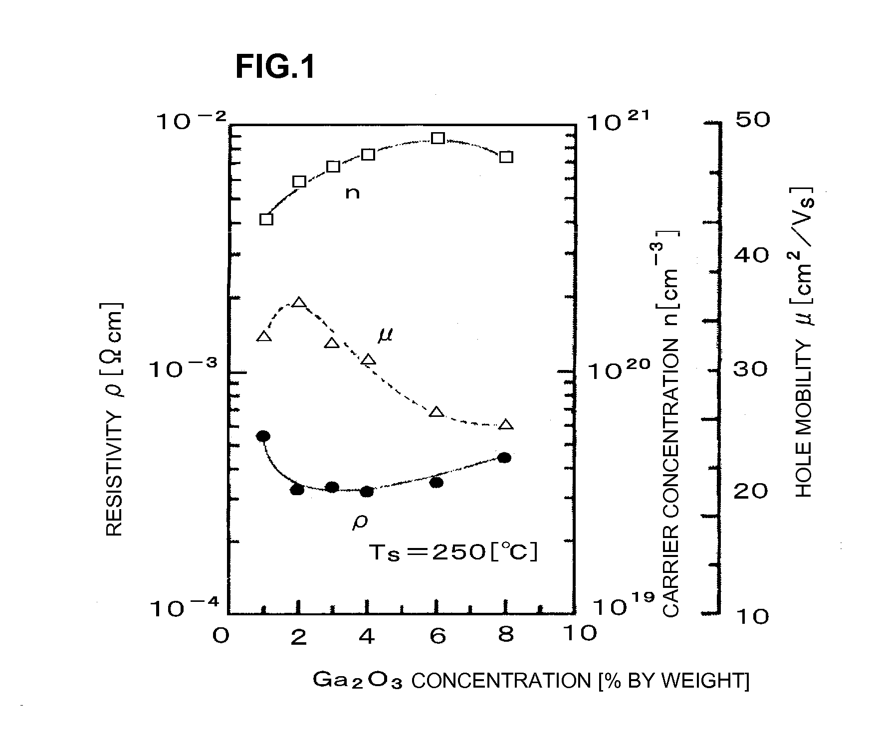
[0118]In Example 1, the Ga2O3 pellets were placed on an erosion region of the ZnO sintered target and subjected to sputtering to form a Ga2O3-doped ZnO film on the substrate.
[0119]The amount of Ga2O3 doping was controlled by controlling the number of the Ga2O3 pellets.
[0120]In the sputtering, the glass substrate was set in a vacuum chamber of a sputtering apparatus and then sputtering was performed without heating of the glass substrate (substrate) after the chamber was evacuated to 5×10⁻⁵ Pa.
[0121]In Example 1, high-purity Ar gas ...
example 2
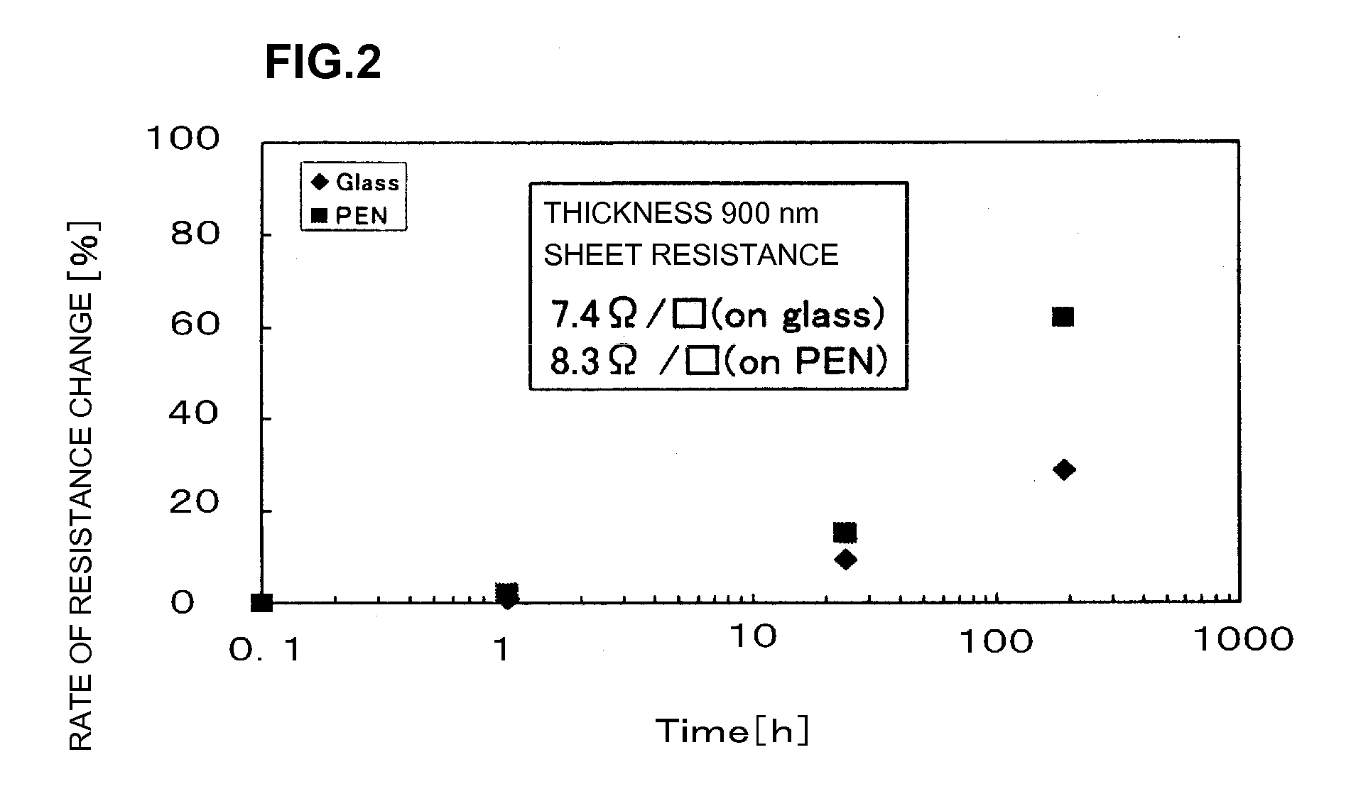
[0171]In Example 1, description is made of the case in which the glass substrate was preferably used as the substrate on which the transparent conductive film was formed. However, in Example 2, a substrate (flexible substrate) composed of PEN (polyethylene naphthalate) was preferably used as a substrate on which a transparent conductive film was formed, and the substrate was pre-treated by the same method as in Example 1.
[0172]Like in Example 1, a ZnO sintered target having a sintering density of 80% or more and a diameter of 6 inches was prepared as a sputtering target.
[0173]Like in Example 1, doping pellets (Ga2O3 pellets) composed of a Ga oxide (Ga2O3) and having a diameter of 10 mm were prepared.
[0174]In Example 2, the Ga2O3 doping amount was controlled by controlling the number of the Ga2O3 pellets.
[0175]Sputtering was performed by the same method using the same sputtering apparatus under the same conditions as in Example 1 to form a Ga-doped ZnO film (transparent conductive fi...
example 3
[0192]A Ga-doped ZnO film (transparent conductive film) was formed by the same sputtering method under the same conditions as in Example 2 except that a substrate (flexible substrate) composed of PET (polyethylene terephthalate) was preferably used instead of the substrate (flexible substrate) composed of PEN (polyethylene naphthalate) used in Example 2.
[0193]As a result of the measurement of the characteristics of the resulting ZnO film (transparent conductive film) under the same conditions as in Example 2, it was confirmed that the ZnO film (transparent conductive film) has the same characteristics as in Example 2.
[0194]It was thus confirmed that a practicable transparent conductive film can be formed on a substrate (flexible substrate) composed of general-purpose PET (polyethylene terephthalate).
PUM
| Property | Measurement | Unit |
|---|---|---|
| pressure | aaaaa | aaaaa |
| resistivity | aaaaa | aaaaa |
| RH | aaaaa | aaaaa |
Abstract
Description
Claims
Application Information


