
Substrate-processing method and method of manufacturing electronic device

a technology of electronic devices and substrates, applied in the direction of instruments, photomechanical devices, optics, etc., can solve the problems of excessive processing time, attention not paid to the index that should be controlled,

Inactive Publication Date: 2008-03-06
KK TOSHIBA
View PDF7 Cites 0 Cited by
  • Summary
  • Abstract
  • Description
  • Claims
  • Application Information

AI Technical Summary

Problems solved by technology

However, in the related art utilizing Caro's acid quoted above and the related art disclosed in the Japanese patent document quoted above, the method for directly measuring the concentration of the Caro's acid has not yet been established and, thus, attentions are not paid to the index that should be controlled.
Such being the situation, an excessively long processing time was required for cleaning the substrate surface by removing the organic material from the surface of the substrate.

Method used


Image

  • Substrate-processing method and method of manufacturing electronic device
  • Substrate-processing method and method of manufacturing electronic device
  • Substrate-processing method and method of manufacturing electronic device

Examples


example 1

[0068]

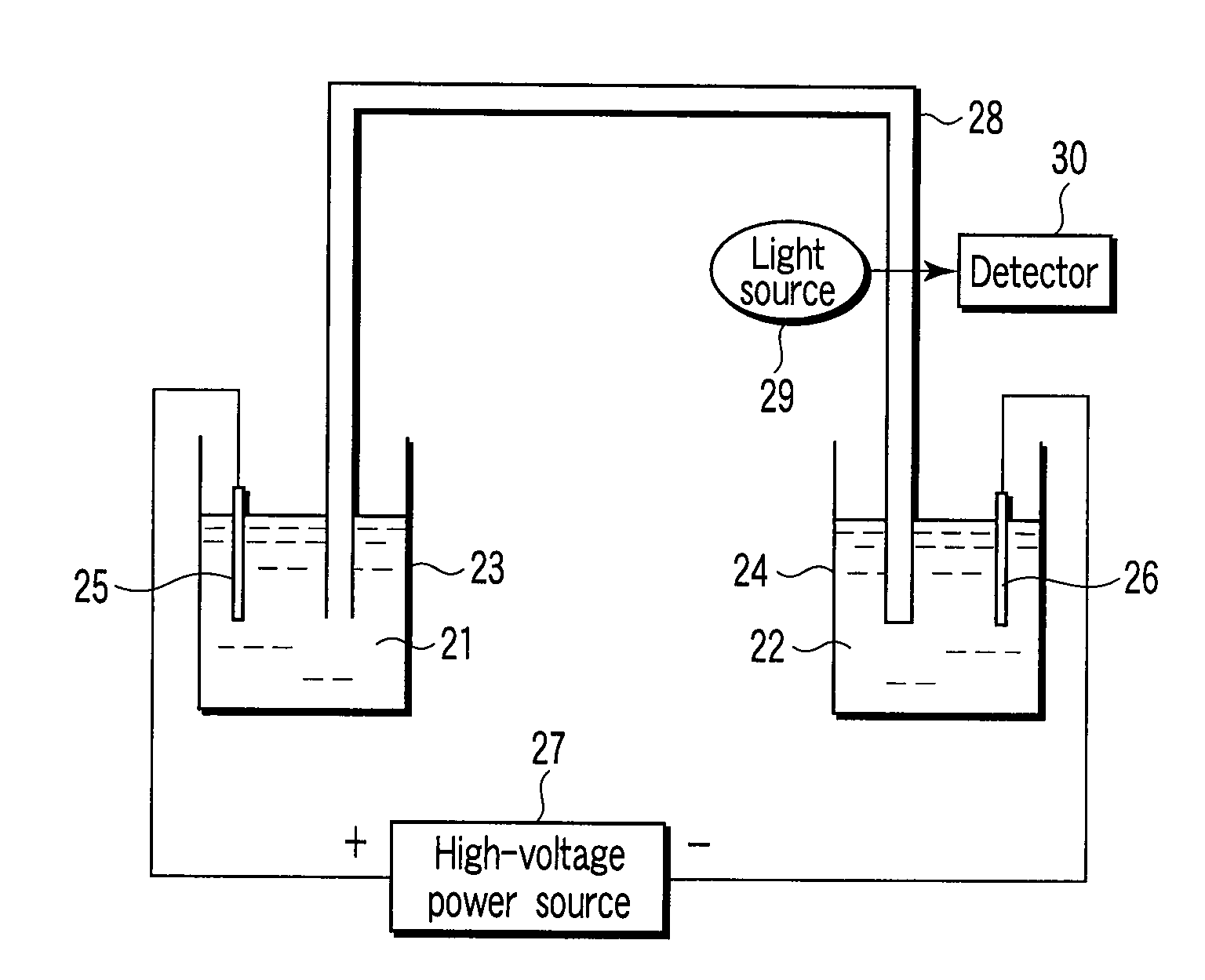
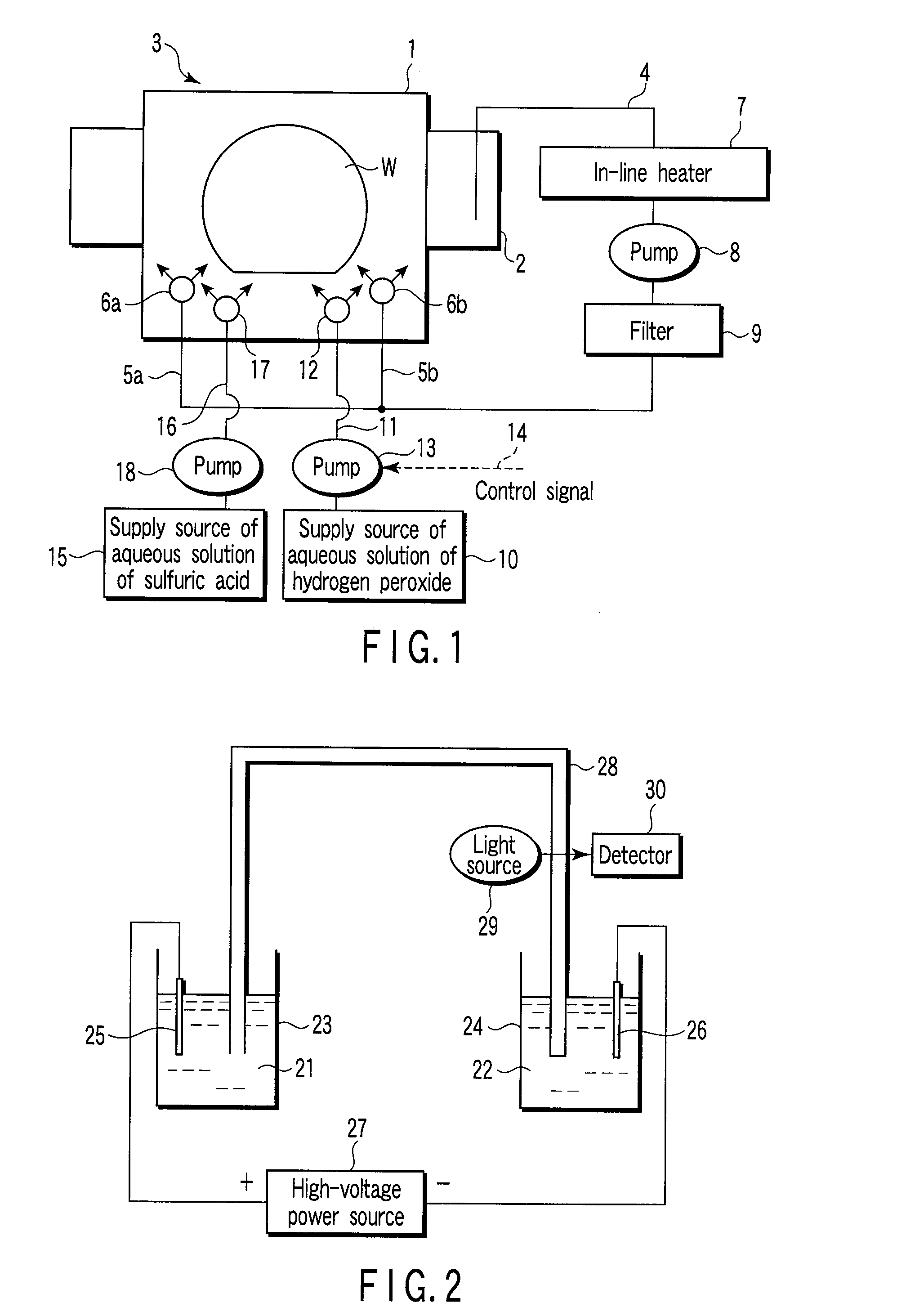
[0069]Solutions were prepared by dissolving in a distilled water quinolinic acid, hexadecyl trimethyl ammonium hydroxide (10% aqueous solution) and 2-amino-2-hydroxymethyl-1,3-propane diol. The solutions thus prepared were used as buffer solutions 21 and 22, respectively, so as to be accommodated in the anode vessel 23 and the cathode vessel 24 of the apparatus shown in FIG. 2. Then, a sample was prepared by mixing an aqueous solution containing 96 to 98% by weight of sulfuric acid with another aqueous solution containing 35% by weight of hydrogen peroxide. In mixing these two aqueous solutions for preparing the sample, the mixing ratio by weight was set at 1:1. The sample thus prepared was mixed with the buffer solution 21 accommodated in the anode vessel 23. Then, a DC voltage of −10 kV, −18 μA was applied from the high voltage power source 27 to the anode plate 25 and the cathode plate 26. After application of the DC voltage, the capillary tube 28 was irradiated with an ult...


PUM

PropertyMeasurementUnit
Fractionaaaaaaaaaa
Particle sizeaaaaaaaaaa
Concentrationaaaaaaaaaa

Abstract

A method of manufacturing an electronic device includes dipping a substrate in a solution containing sulfuric acid, which is accommodated in a processing vessel. An aqueous solution of hydrogen peroxide supplies the sulfuric acid accommodated in the processing vessel for generating peroxomonosulfuric acid (Caro's acid). Therefore, an organic material present on the surface of the substrate is removed by the action of Caro's acid within the processing vessel. The time for supplying the aqueous solution of hydrogen peroxide into the processing vessel is set on the basis of the change with time in the concentration of Caro's acid measured in advance so as to permit the peak in the concentration of Caro's acid to appear while the substrate is kept dipped in the processing solution.

Description

CROSS-REFERENCE TO RELATED APPLICATIONS[0001]This application is based upon and claims the benefit of priority from prior Japanese Patent Application No. 2006-235311, filed Aug. 31, 2006, the entire contents of which are incorporated herein by reference.BACKGROUND OF THE INVENTION[0002]1. Field of the Invention[0003]The present invention relates to a method of processing a substrate such as a silicon wafer and a glass substrate for a display device and to a method of manufacturing an electronic device such as a semiconductor device or a display device, particularly, relates to the technique for removing an organic material such as a photoresist material from a substrate.[0004]2. Description of the Related Art[0005]In the manufacture of an electronic device such as a semiconductor device, various films such as a conductive film and an insulating film are formed on a substrate, followed by forming a resist pattern on the films formed on the substrate and subsequently removing selectiv...

Claims


Application Information

Patent Timeline
IPC IPC(8): C23G1/02
CPCH01L21/67086G03F7/423
Inventor SHIBATA, YUKIHIROHAYAMIZU, NAOYA
Owner KK TOSHIBA
Learn More