

Semiconductor chip and method for fabricating the same
a semiconductor and chip technology, applied in the field of semiconductor chips, can solve the problems of poor elastic buffer, easy cracking between the conventional gold bump and the acf, and the possibility of refractive light through the glass substrate, etc., and achieve the effect of saving the cost of forming
- Summary
- Abstract
- Description
- Claims
- Application Information
AI Technical Summary
Benefits of technology
Problems solved by technology
Method used
Image

Examples
embodiment 1
Aspect 5 of Embodiment 1
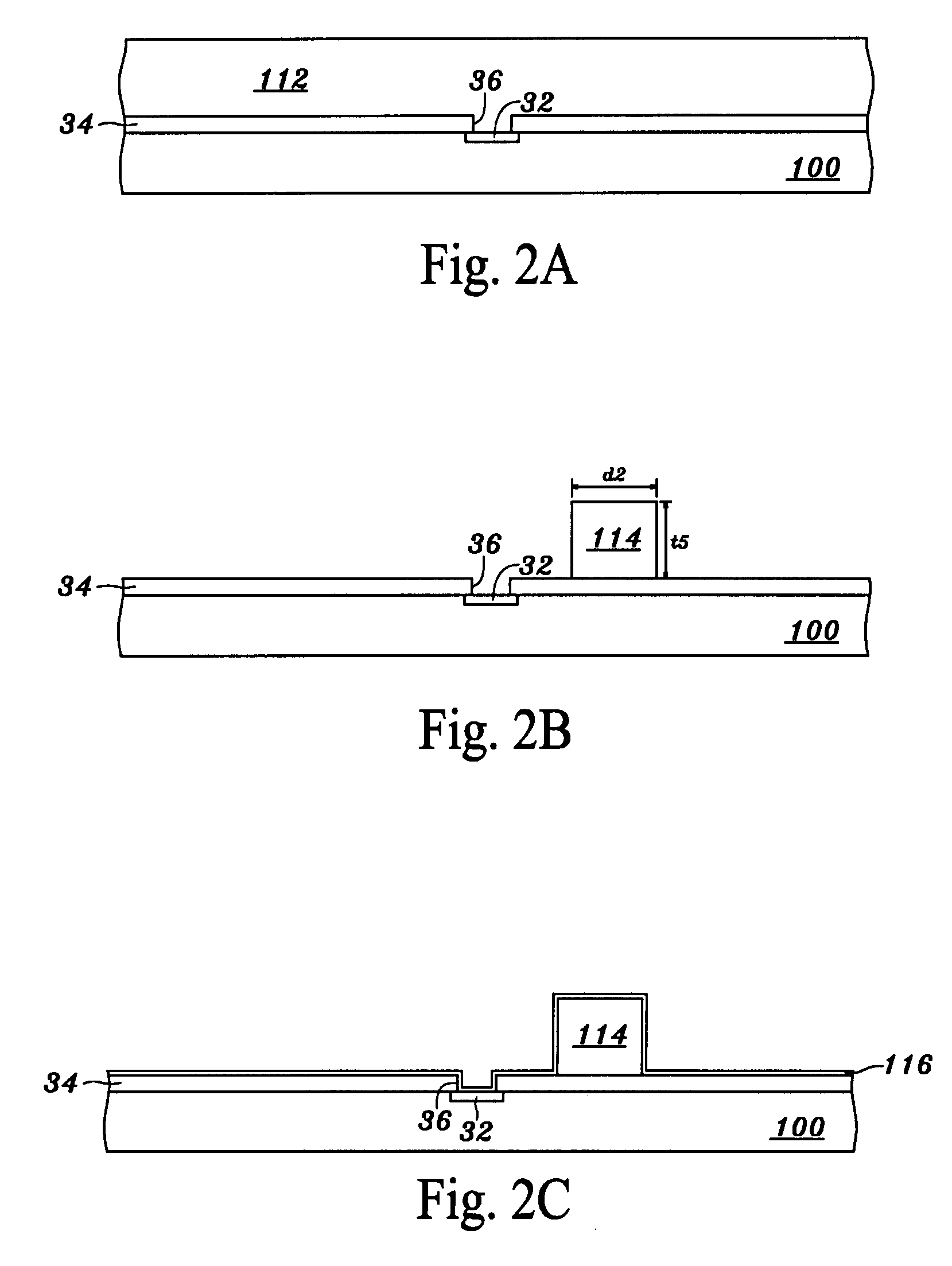
[0109]Referring to FIG. 6A, after the step shown in FIG. 5A is completed, the polymer layer 112 is patterned with exposure and development processes to form at least one polymer bump 114 on the passivation layer 34, and to form at lest one polymer island 148 on the passivation layer 34, an opening 148a in the polymer island 148 exposing the pad 32′, and the pad 32 being uncoved by the polymer bump 114 and the polymer island 148. From a top perspective view, the position of the polymer bump 114 is different from that of the pad 32.
[0110]The pad 32′ may include a center portion exposed by the opening 148a and a peripheral portion covered with the polymer island 148, as shown in FIG. 6A. Alternatively, the opening 148a may expose the entire upper surface of the pad 32′ exposed by the opening 36 in the passivation layer 34 and further may expose the upper surface of the passivation layer 34 near the pad 32′.
[0111]The material of the polymer bump 114 and the polym...
embodiment 2
Aspect 4 of Embodiment 2
[0164]Referring to FIGS. 10A and 10B, after the step shown in FIG. 5A is completed, the polymer layer 112 is patterned with exposure and development processes to form a polymer bump 114 on a portion of the pad 32 exposed by the opening 36 and on the passivation layer 34 close to the pad 32, and to form a polymer island 148 on the passivation layer 34, an opening 148a in the polymer island 148 exposing the pad 32′. The top surface of the pad 32 exposed by the opening 36 may have a first region 152 uncovered by the polymer bump 114 and a second region covered by the polymer bump 114. The ratio of the area of the first region 152 to that of the pad 32 is between 0.1 and 0.9, or between 0.05 and 0.5.
[0165]The pad 32′ may include a center portion exposed by the opening 148a and a peripheral portion covered with the polymer island 148, as shown in FIG. 10A. Alternatively, the opening 148a may expose the entire upper surface of the pad 32′ exposed by the opening 36 ...
embodiment 3
Aspect 3 of Embodiment 3
[0216]Referring to FIG. 13A, after the step shown in FIG. 12D is completed, a photoresist layer 120, such as positive-type photoresist layer, having a thickness of between 6 and 100 μm, and preferably of between 10 and 50 μm, is spin-on coated on the seed layer 118. Next, the photoresist layer 120 is patterned with exposure and development processes to form an opening 120a in the photoresist layer 120 exposing the seed layer 118 over the top surface of the polymer bump 114, at the sidewall(s) of the opening 114a, and over the center region 32a of the pad 32, and to form an opening 120b in the photoresist layer 120 exposing the seed layer 118 over the passivation layer 34 and over the pad 32′. A 1X stepper or 1X contact aligner can be used to expose the photoresist layer 120 during the process of exposure. The process of forming the photoresist layer 120 and the openings 120a and 120b, as shown in FIG. 13A, can be referred to as the process of forming the phot...
PUM
| Property | Measurement | Unit |
|---|---|---|
| width | aaaaa | aaaaa |
| width | aaaaa | aaaaa |
| thickness | aaaaa | aaaaa |
Abstract
Description
Claims
Application Information