Thermal processing system for curing dielectric films

a dielectric film and processing system technology, applied in the direction of vacuum evaporation coating, electric/magnetic/electromagnetic heating, coatings, etc., can solve the problems of limiting interconnection delay, mechanical strength deterioration, and low-k materials less robust than more traditional silicon dioxide, so as to facilitate the treatment process

Inactive Publication Date: 2008-03-13
TOKYO ELECTRON LTD
View PDF56 Cites 122 Cited by
  • Summary
  • Abstract
  • Description
  • Claims
  • Application Information

AI Technical Summary

Benefits of technology

[0013]Any of these and/or other aspects may be provided by a processing system for treating a dielectric film in accordance with the present invention. In one embodiment, the processing system for treating a dielectric film on a substrate includes: a process chamber configured to facilitate the treatment process; a substrate holder coupled to the process chamber, and configured to support the substrate in the process chamber; a temperature control system coupled to the substrate holder and configure...

Problems solved by technology

As is known to those in the semiconductor art, interconnect delay is a limiting factor in the drive to improve the speed and performance of integrated circuits (IC).
Low-k materials are less robust than more traditional silicon dioxide, and the mechanical strength deteriorates further with the introduction of porosity.
The porous low-k films can easily be damaged during plasma processing, thereby making desirable a mechanical strengthening process.
However, when processing porous dielectric films (such as ultra low-k films) with a high le...

Method used


Image

  • Thermal processing system for curing dielectric films
  • Thermal processing system for curing dielectric films
  • Thermal processing system for curing dielectric films

Examples


Embodiment Construction

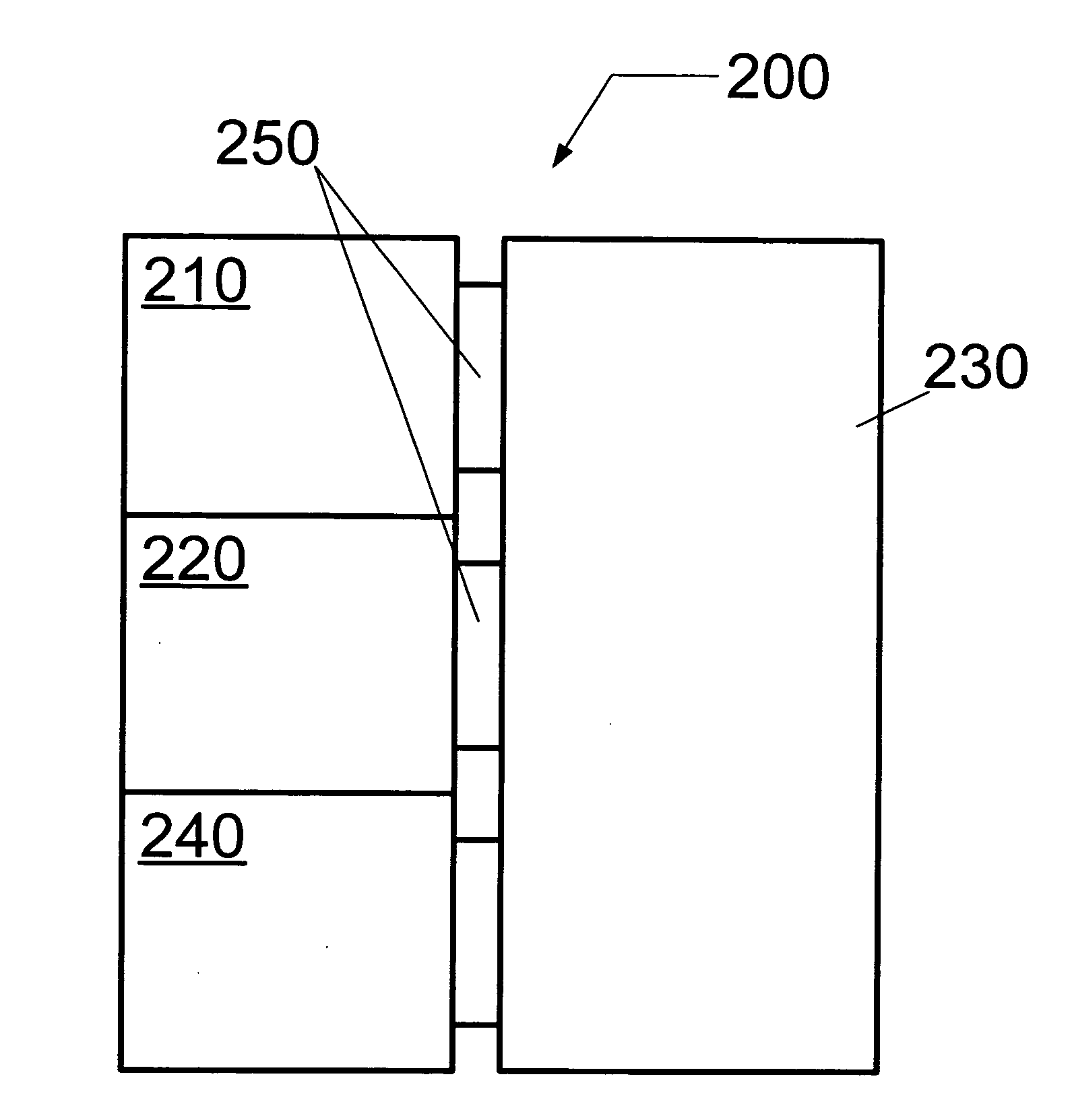
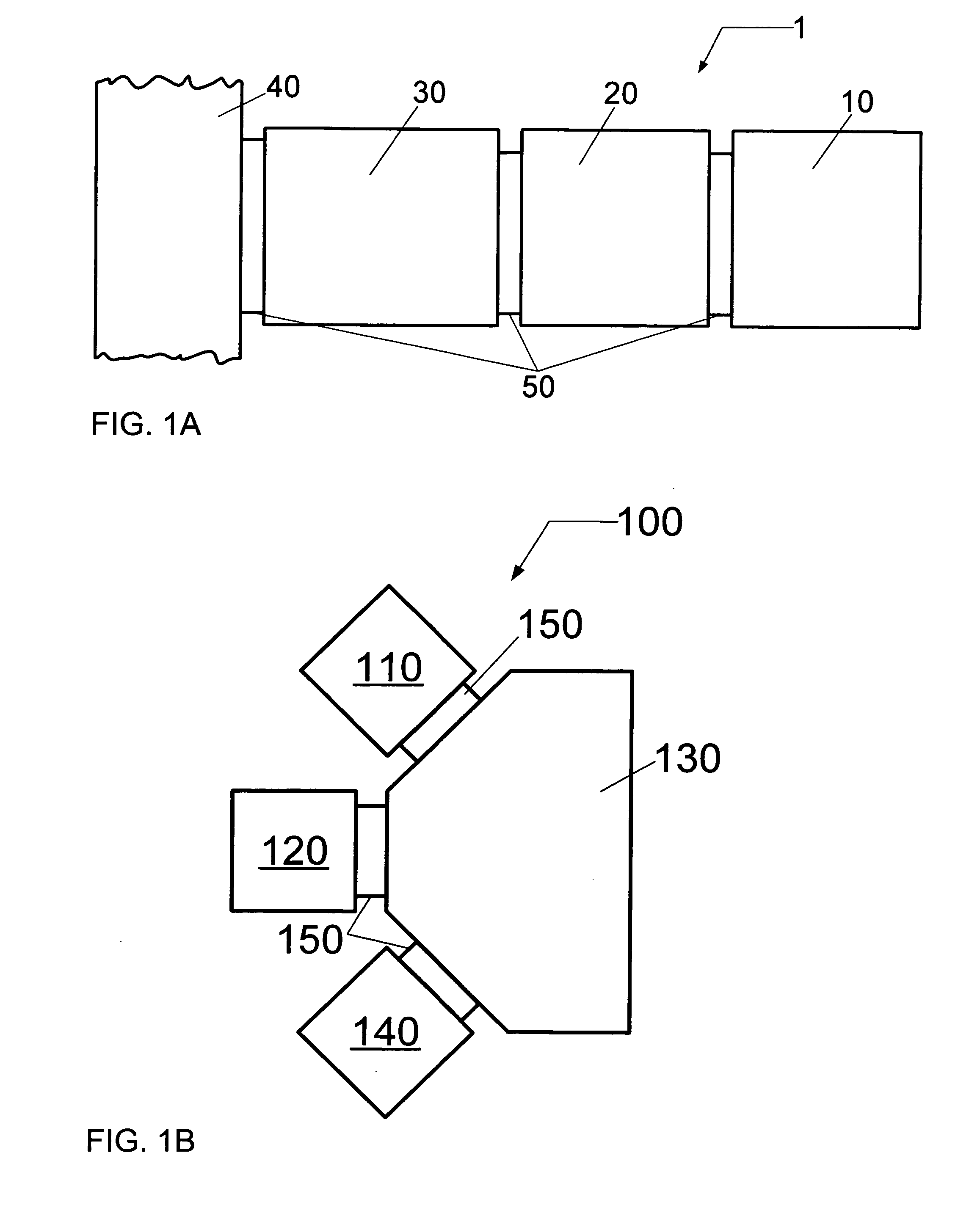
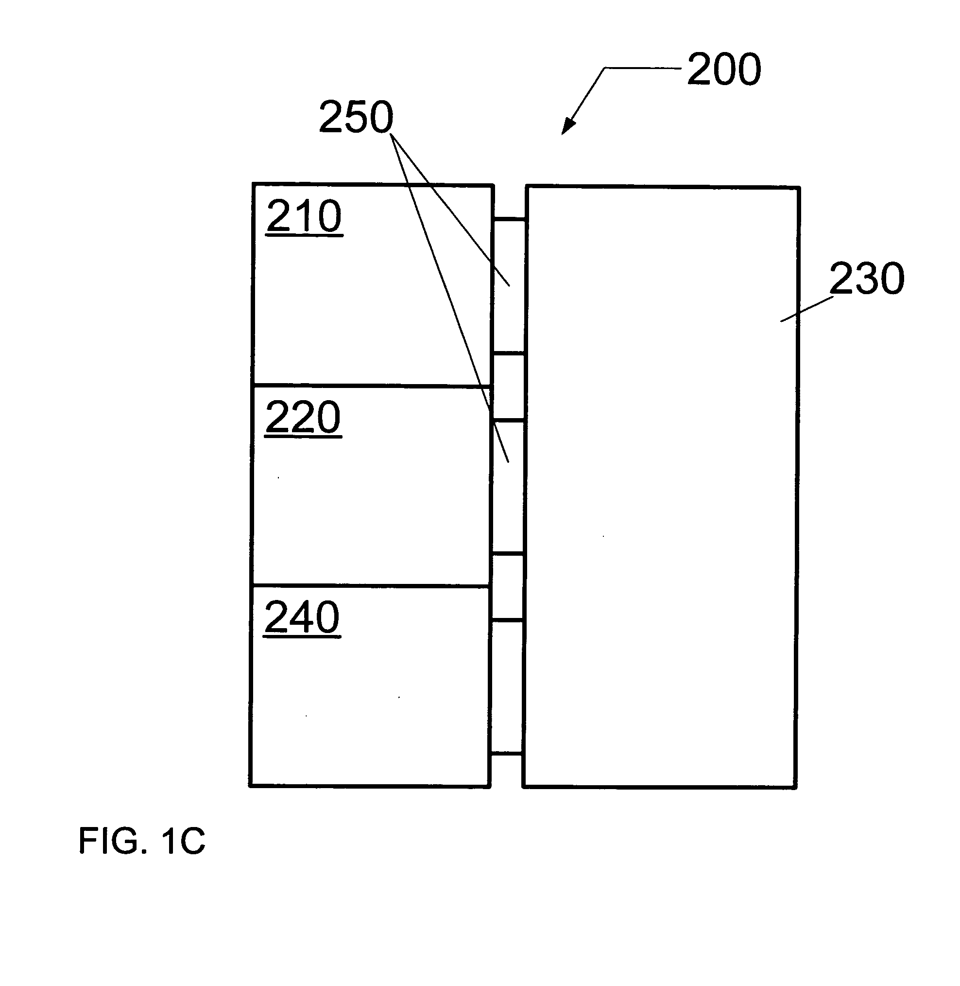
[0021]In the following description, in order to facilitate a thorough understanding of the invention and for purposes of explanation and not limitation, specific details are set forth, such as a particular geometry of the processing system and descriptions of various components. However, it should be understood that the invention may be practiced in other embodiments that depart from these specific details.

[0022]The present invention recognized that alternative curing methods address some of the deficiencies of thermal curing. For instance, alternative curing methods are more efficient in energy transfer, as compared to thermal curing processes, and the higher energy levels found in the form of energetic particles, such as accelerated electrons, ions, or neutrals, or in the form of energetic photons, can easily excite electrons in a low-k film, thus efficiently breaking chemical bonds and dissociating side groups. These alternative curing methods facilitate the generation of cross-l...


PUM

PropertyMeasurementUnit
Temperatureaaaaaaaaaa
Lengthaaaaaaaaaa

Abstract

A thermal processing system and method for curing a dielectric film. The thermal processing system is configured to treat the dielectric film with ultraviolet (UV) radiation and infrared (IR) radiation in order to cure the dielectric film. The thermal processing system can include an array if IR and UV light-emitting devices (LEDs) configured to irradiate a substrate having a low dielectric constant (low-k) film. The method dries the dielectric film to remove contaminants from the film and exposes the dielectric film at a single stage to ultraviolet radiation and IR radiation.

Description

BACKGROUND OF THE INVENTION[0001]1. Field of the Invention[0002]The present invention relates to a system for treating a dielectric film and, more particularly, to a system for curing a dielectric film using infrared (IR) and ultraviolet (UV) radiation.[0003]2. Description of Related Art[0004]As is known to those in the semiconductor art, interconnect delay is a limiting factor in the drive to improve the speed and performance of integrated circuits (IC). One way to minimize interconnect delay is to reduce interconnect capacitance by using low dielectric constant (low-k) materials as the insulating dielectric for metal wires in the IC devices. Thus, in recent years, low-k materials have been developed to replace relatively high dielectric constant insulating materials, such as silicon dioxide. In particular, low-k films are being utilized for inter-level and intra-level dielectric layers between metal wires in semiconductor devices. Additionally, in order to further reduce the diele...

Claims


Application Information

Patent Timeline
IPC IPC(8): B05D3/06C23C14/28B05B5/025
CPCH01L21/3105H01L21/31058H01L21/67115H01L21/31695H01L21/31612H01L21/02126H01L21/02271H01L21/02134H01L21/02203H01L21/02282H01L21/02137H01L21/02345H01L21/02348
Inventor LEE, ERIC M.LIU, JUNJUN
Owner TOKYO ELECTRON LTD
Why Eureka
Try Eureka