Water-based polishing pads having improved contact area

a technology of polishing pads and water-based solutions, which is applied in the field of polishing pads, can solve the problems of cumbersome (organic) solvents that are typically used (e.g., n,n-dimethyl formamide) and cost prohibitive handling, and can have center-to-edge variations in density and porosity within the pads

Inactive Publication Date: 2008-03-13
ROHM & HAAS ELECTRONICS MATERIALS CMP HLDG INC
View PDF9 Cites 19 Cited by
  • Summary
  • Abstract
  • Description
  • Claims
  • Application Information

AI Technical Summary

Problems solved by technology

Unfortunately, polyurethane pads produced from the casting and skiving method can have polishing variations arising from a polishing pad's casting location.
Furthermore, polishing pads cut from molds of excessive size can have center-to-edge variations in density and porosity within a pad.
These variations can adversely affect polishing for the most demanding applications, such as low k patterned wafers.
Unfortunately, the (organic) solvent that is typically used (e.g., N,N-dimethyl formamide) may be cumbersome and cost prohibitive to handle.
In addition, these soft pads may suffer from pad-to-pad variations due to the random placement and structure of the porosities that are formed during the coagulation process.
Unfortunately, the higher down force pressures may exhibit a greater amount of defectivity in the polished article.

Method used


Image

  • Water-based polishing pads having improved contact area
  • Water-based polishing pads having improved contact area
  • Water-based polishing pads having improved contact area

Examples


examples

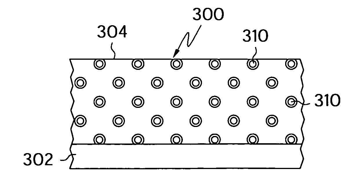
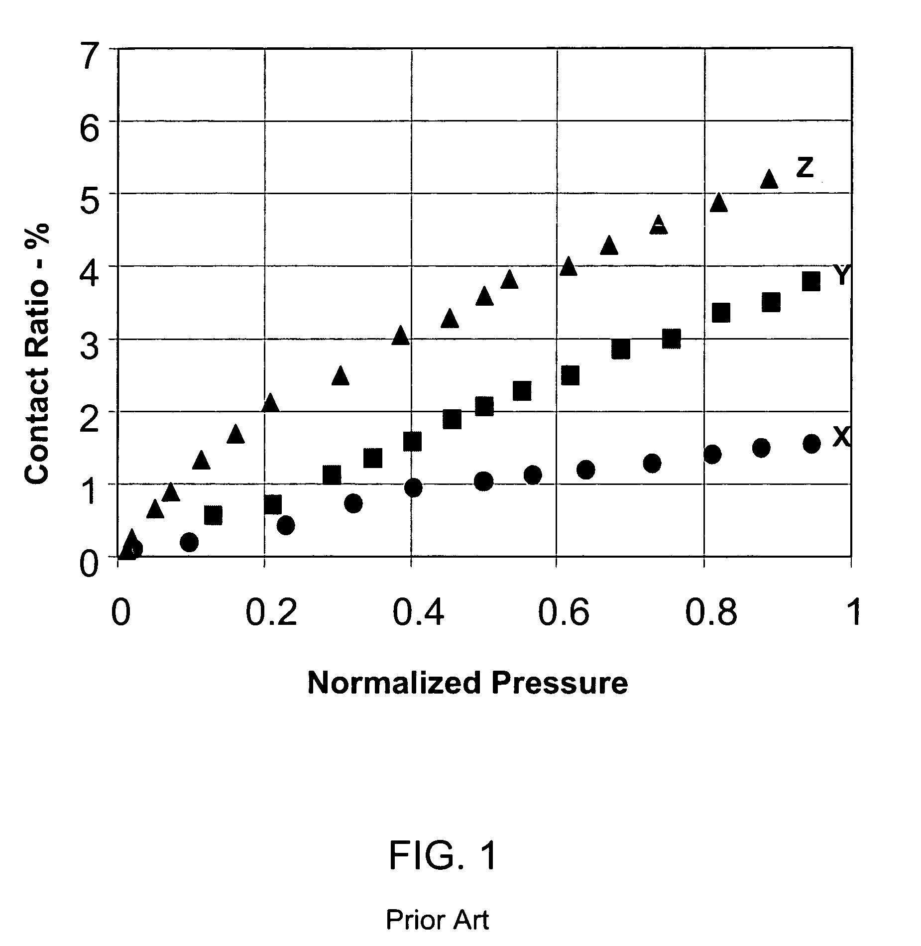
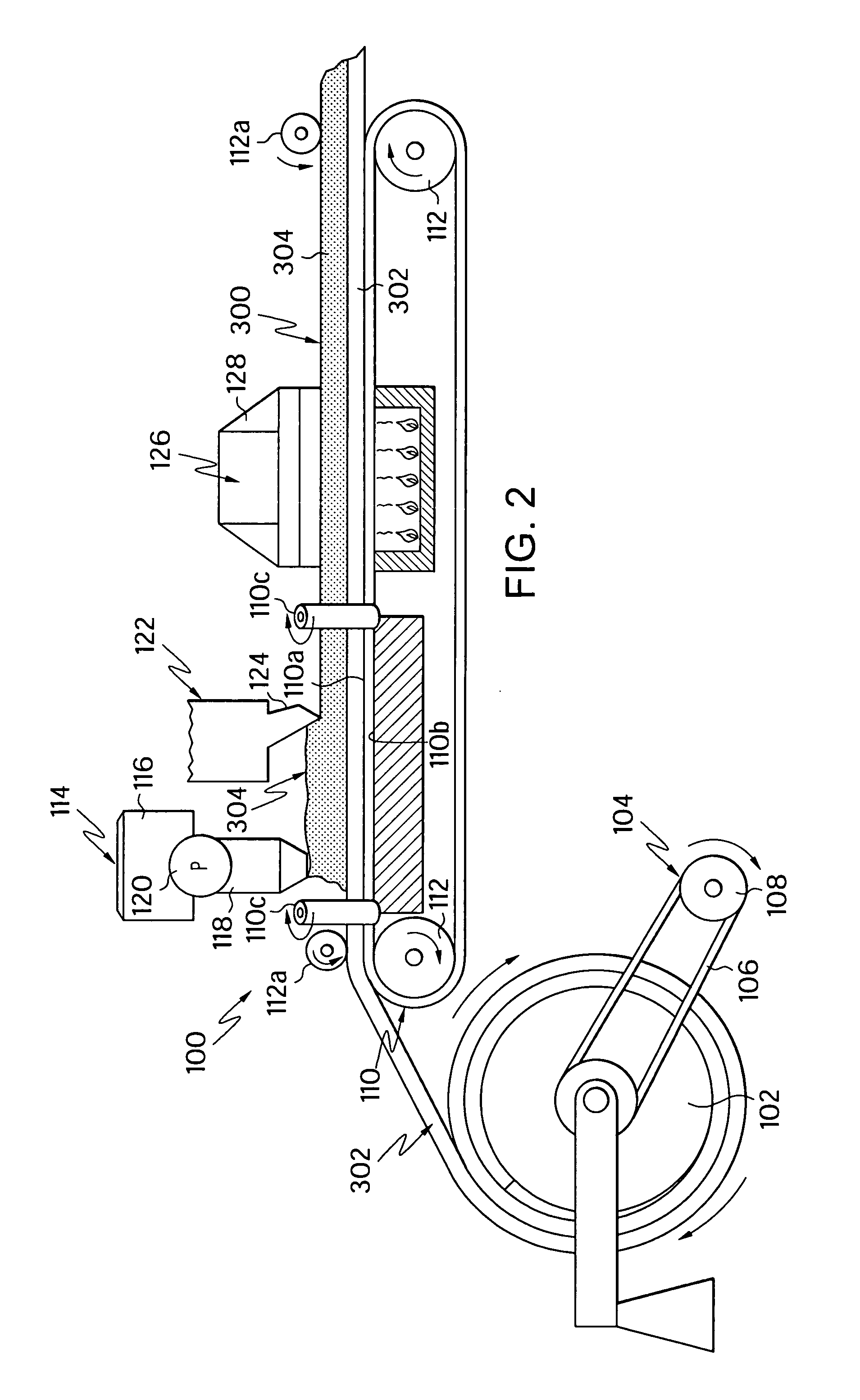
[0053]The following Table illustrates the improved defectivity of the water-based pad of the present invention. The water-based pad was formed by mixing 75 grams of W-290H from Crompton Corp. with 25 grams of Rhoplex® E-358 from Rohm and Haas Company in a 3 to 1 ratio for 2 minutes in a mix tank. Then, 1 gram of Foamaster® 111 from Cognis was added to the mix tank and mixed for another 2 minutes. Then 0.923 grams of Expancel® 551 DE40d42 (Expancel® 551DE40d42 is a 30-50 μm weight average diameter hollow-polymeric microsphere manufactured by Akzo Nobel) was added to the mix tank and mixed for another 5 minutes. Also, 1 gram of a thickener, Acrysol® ASE-60 and 5 Acrysol I-62, both from Rohm and Haas Company was added to the mix tank and mix for 15 minutes. Then, the mixture was coated (50 mils (1.27 mm) thick wet) on a 453 PET film from Dupont Teijin and dried in a hot air oven at 60° C. for 6 hrs. The resulting polishing pad was 25 mils (0.64 mm) thick. The water-based polishing pad ...


PUM

PropertyMeasurementUnit
volume percentaaaaaaaaaa
thickaaaaaaaaaa
weight average diameteraaaaaaaaaa

Abstract

The present invention provides a chemical mechanical polishing pad comprising, a polymeric matrix having microspheres dispersed therein, the polymeric matrix being formed of a water-based polymer or blends thereof, wherein the pad comprises: a Shore A hardness of 30 to 70; a void volume fraction of 0.2 to 80 percent; a tensile strength of 1 mPa to 5 mPa; and a percent elongation of 200 to 400.

Description

BACKGROUND OF THE INVENTION[0001]The present invention relates to polishing pads for chemical mechanical planarization (CMP), and in particular, relates to water-based polishing pads having improved percent contact area.[0002]In the fabrication of integrated circuits and other electronic devices, multiple layers of conducting, semiconducting and dielectric materials are deposited on or removed from a surface of a semiconductor wafer. Thin layers of conducting, semiconducting, and dielectric materials may be deposited by a number of deposition techniques. Common deposition techniques in modern processing include physical vapor deposition (PVD), also known as sputtering, chemical vapor deposition (CVD), plasma-enhanced chemical vapor deposition (PECVD), and electrochemical plating (ECP).[0003]As layers of materials are sequentially deposited and removed, the uppermost surface of the wafer becomes non-planar. Because subsequent semiconductor processing (e.g., metallization) requires th...

Claims


Application Information

Patent Timeline
Patent Type & Authority Applications(United States)
IPC IPC(8): B32B5/22
CPCB24B37/24Y10T428/24504Y10T428/24537Y10T428/249986
Inventor DUONG, CHAU H.
Owner ROHM & HAAS ELECTRONICS MATERIALS CMP HLDG INC
Why Eureka
Try Eureka