
Electron Beam Holography Observation Apparatus

Inactive Publication Date: 2008-03-20
HITACHI LTD
View PDF11 Cites 7 Cited by
  • Summary
  • Abstract
  • Description
  • Claims
  • Application Information

AI Technical Summary

Benefits of technology

[0019]In the light of the above problems, the present invention has for its object to provide realization of easy-to-handle holography observation for enabling a wide range of persons from beginners to skilled persons to operate an electron microscope in the course of holography observation.
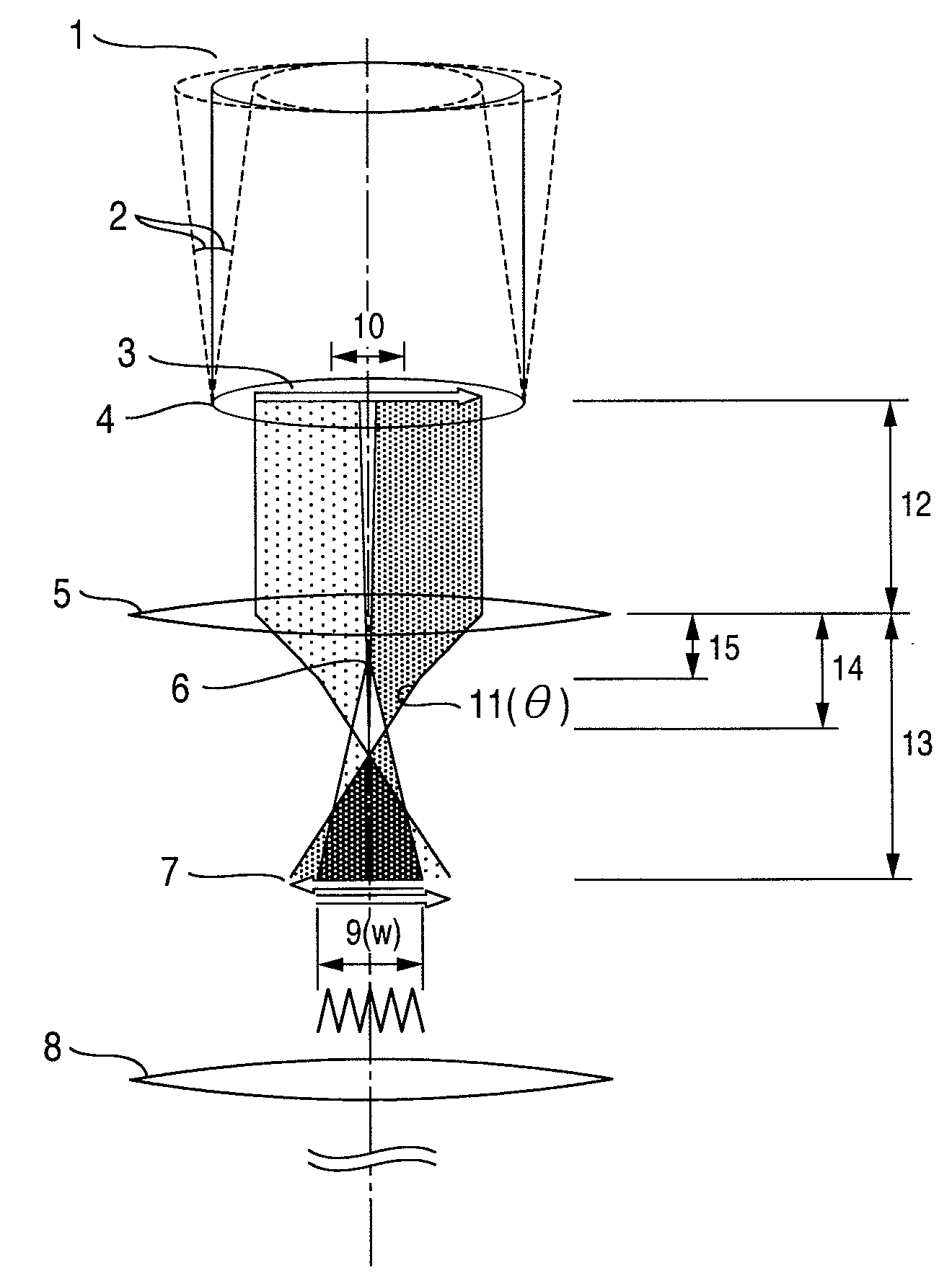
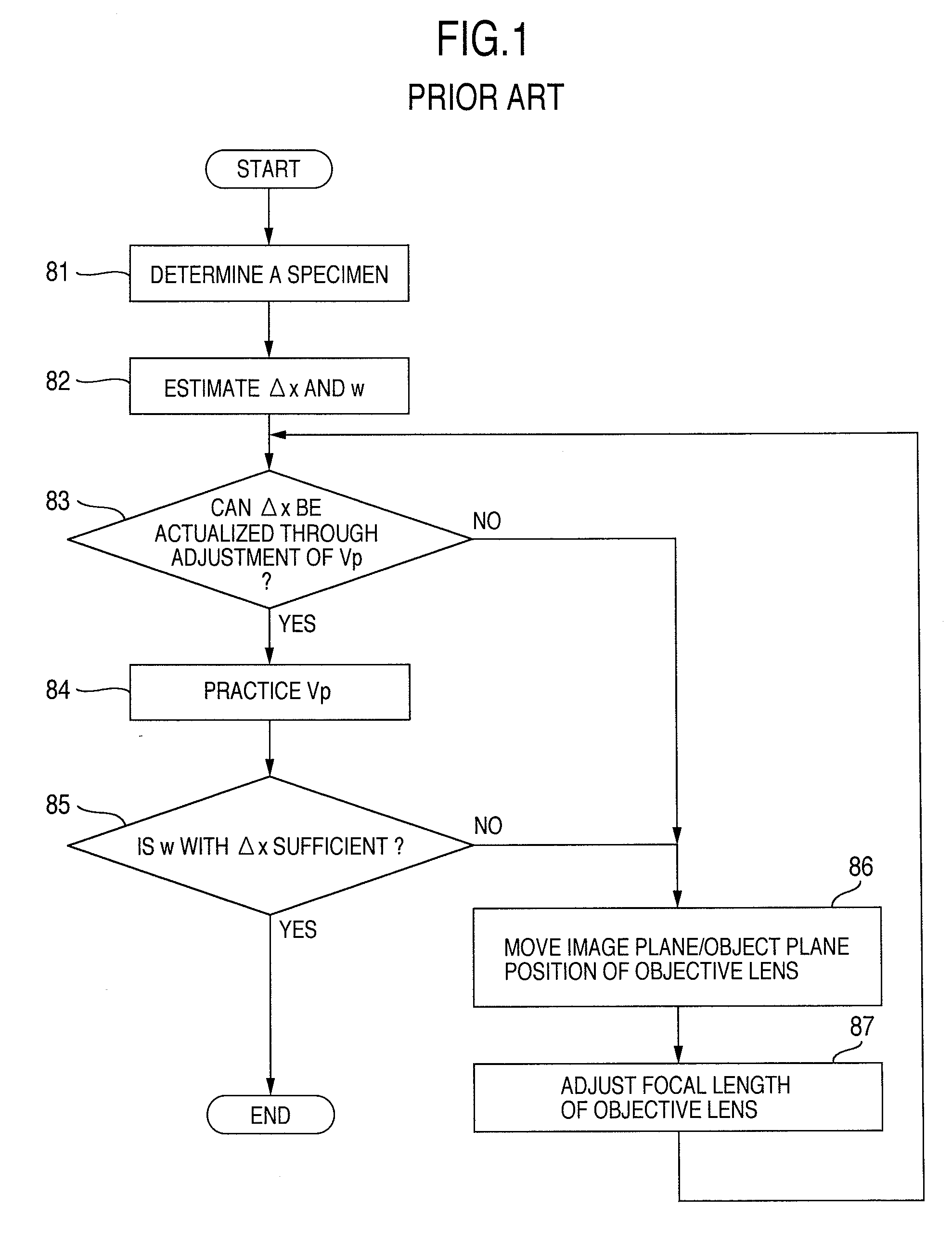
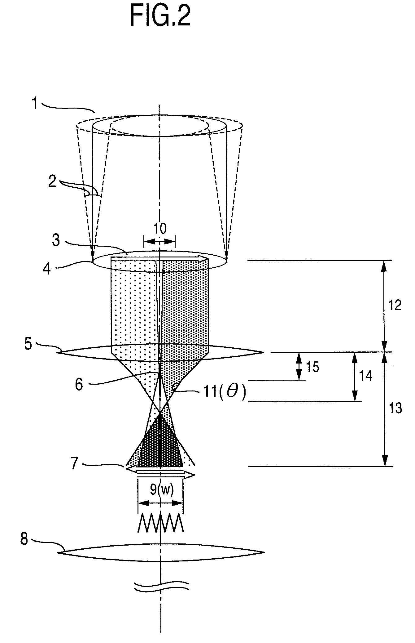
[0020]In an electron microscope capable of performing holography observation, a mechanism for up-down moving one of a specimen position and an electron biprism position or both in at least the optical axis direction is provided and an information processing unit having the function to automatically calculate the amount of movement is also provided. Further, the information processing unit has the function to examine whether the specimen position or the electron biprism position after movement has a proper value to realize a spatial resolution or an interference area size an device user desires, thus alleviating a load imposed on the device user during adjustment for observation.
[0021]According to the present invention, upon conducting holography observation with the electron microscope, positions of electron biprism and specimen necessary to realize a requested spatial resolution or interference area are determined by a calculation unit and besides, the electron biprism and specimen positions are moved toward the respective calculated position targets. In this process, the condition for holography observation can be set semi-automatically. Consequently, the time required for searching the observation condition, listed as the problematic issue encountered in the holography observation with the conventional electron microscope, can be reduced.

Problems solved by technology

In spite of the fact that the electron holography is known as a useful analysis method, it is practiced almost in laboratories at present and cannot be said to be materialized in the form of a device widely used as analysis appliance for practical purposes.
To describe more specifically, the use purpose of the device quite differs depending on device users and hence conditions of wide range having difficulties in generalization must be covered, bottlenecking automation of the electron optical condition setting and besides, most of device users are skilled persons such as researchers who are prone to customize the device from the viewpoint of hardware and software and so manual operation meets user's needs rather than relying on low-grade automation.
Therefore, in many cases, adjustment of the amounts of intermediate lens current is difficult to execute on the user side and even if an adjustment of the current amount has been done, a fine change amount adjustment is often impossible in effect.
Therefore, the conventional device fails to realize enlargement or narrowness of the interference fringe spacing while keeping an interference area increased in excess of a constant limit.
Accordingly, a highly graded technical level is required for adjustment and persons other than operators very skilled in electron microscope operation are forced to confront extremely sophisticated work.

Method used


Image

  • Electron Beam Holography Observation Apparatus
  • Electron Beam Holography Observation Apparatus
  • Electron Beam Holography Observation Apparatus

Examples


embodiment 1

[0032]In the present embodiment, an example will be described in which a holography electron method of the present invention is applied to a transmission electron microscope (TEM).

[0033]The transmission electron microscope in the present embodiment is externally configured as schematically illustrated in FIG. 3. The transmission electron microscope shown in FIG. 3 generally comprises an electron microscope column 37, a stand 38 on which the electron microscope column 37 is mounted, a power supply unit 36 for supplying voltage or current to individual components of the electron microscope column 37, a television monitor 32 for displaying picked-up TEM images and a controller 28 for controlling the power supply unit 36.

[0034]The electron microscope column 37 includes an electron gun 16 and underlying illuminating optical system and image forming optical system. The electron gun 16 is comprised of an electron source 17 formed from stylus tungsten single crystal having a sharpened fore ...

embodiment 2

[0070]In the present embodiment, an example will be described in which the present invention is applied to a scanning transmission electron microscope (STEM). The device construction of the STEM incorporating the automatic adjustment function according to the present invention is schematically diagrammatically illustrated in FIG. 9. In the case of the STEM, a deflection coil 70 for scanning a focused electron beam formed by the objective lens 5 on the specimen surface and a scan control power supply 71 are built in. Further, the position of electron biprism 6 differs from that in the TEM so as to be above an illuminating lens 21 but except for the above, constituent elements are substantially the same as those of the device shown in FIG. 3.


PUM


Abstract

In electron holography observation using a transmission electron microscope, searching of conditions of an electron optical condition which are necessary for realizing a requested spatial resolution is sophisticated and for persons unaccustomed to operation of the electron microscope, the observation is time consuming work. In addition to the fundamental electron microscope proper, an input unit for inputting a spatial resolution requested in the holography observation, a calculation unit for calculating positions of electron biprism and specimen necessary for realizing the requested spatial resolution from the inputted value and parameters characteristic of the device and mechanisms for moving the two positions for realizing the obtained calculation results are provided.

Description

INCORPORATION BY REFERENCE[0001]The present application claims priority from Japanese application JP2006-161783 filed on Jun. 12, 2006, the content of which is hereby incorporated by reference into this application.BACKGROUND OF THE INVENTION[0002]The present invention relates to devices for observing an image of a specimen by using a charged particle beam and an observation method using with them and more particularly, to a means for making a optimum optical condition for observation more easier in electron holography method than in a conventional one.[0003]The electron holography method is one of specimen observation methods by an electron microscope. The electron holography method is an observation method utilizing the nature of electrons behaving as a wave, according to which an electron beam having transmitted through a substance (object wave) is interfered with an electron beam unaffected by the substance (reference wave) to obtain an interference fringe and phase information ...

Claims


Application Information

Patent Timeline
IPC IPC(8): G21K7/00
CPCG03H5/00H01J37/147H01J2237/2614H01J2237/1514H01J2237/2487H01J37/26
Inventor KASAI, HIROTOKANEKO, YUTAKA
Owner HITACHI LTD
Learn More