

Charged particle beam apparatus
- Summary
- Abstract
- Description
- Claims
- Application Information
AI Technical Summary
Benefits of technology
Problems solved by technology
Method used
Image

Examples
first embodiment
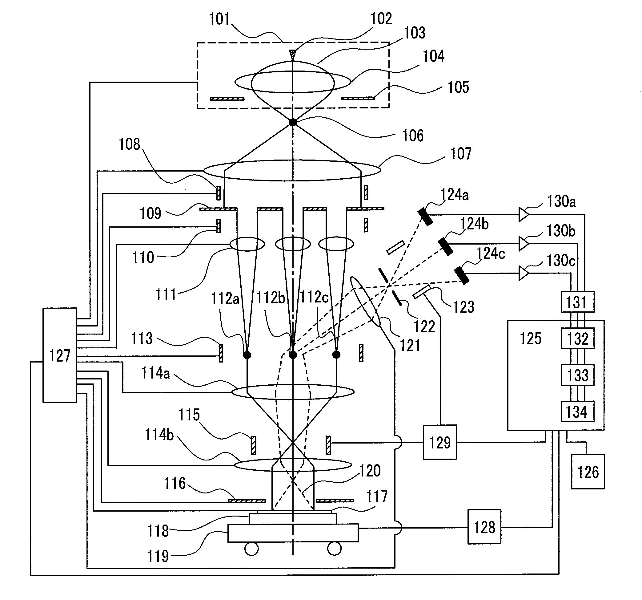
[0030]FIG. 1 is a diagram for showing a schematic configuration of a multi-electron-beam inspection system according to a first embodiment of this invention. This apparatus is broadly divided into a primary electron optics for controlling primary beams (primary charged particle beam) 103 that is emitted from a cathode 102 and reaches the specimen 117, and a secondary electron optics for controlling secondary beams (secondary charged particle beam) 120 produced by interaction between the primary beams and the specimen 117. An alternate long and short dash line denotes an axis with which a symmetry axis of the primary electron optics formed substantially in rotation symmetry should coincide and that serves as a reference of the primary beam path. Hereinafter it is called a central axis.
[0031]An electron gun 101 includes the cathode 102 made of a material whose work function is low, an anode 105 having a high electric potential to the cathode 102, a magnetic lens 104 for superimposing ...
second embodiment
[0058]FIG. 7 is a diagram for showing a schematic configuration of a multi-electron-beam inspection apparatus according to a second embodiment of this invention.
[0059]The electron gun 101 includes the cathode 102 made of a material whose work function is low, the anode 105 having a high electric potential to the cathode 102, the magnetic lens 104 for superimposing a magnetic field on an acceleration electric field formed between the cathode 102 and the anode 105. For the cathode 102, this example uses the Schottky cathode that easily delivers a large electric current and is also stable in electron emission. The primary beam 103 emitted from the cathode 102 is accelerated in a direction of the anode 105, while receiving a focusing action by the magnetic lens 104.
[0060]The reference numeral 106 denotes the first image of source. Using this first image of source 106 as a light source, the condenser lens 107 adjusts the primary beam so as to be substantially collimated. In this embodime...
third embodiment
[0069]FIGS. 11A and 11B are diagrams for explaining a principle in a third embodiment of this invention.
[0070]An alternate long and short dash line is an axis with which a symmetry axis of an objective lens formed in a field of substantially rotation symmetry should coincide, and serves as a standard of a primary beam path. It is hereinafter called the central axis.
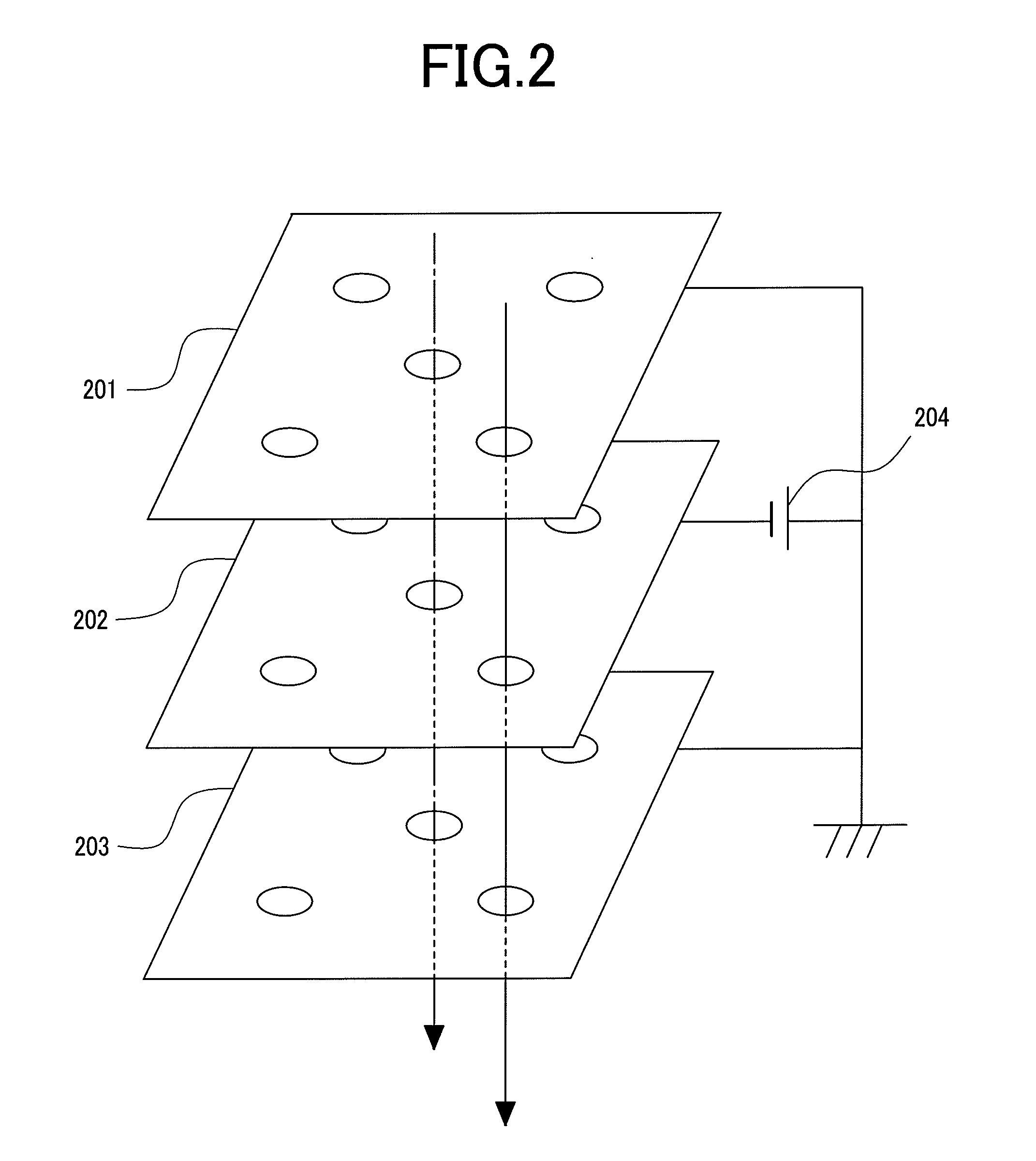
[0071]In FIG. 11A, a plurality of primary beams 1101a, 1101b, and 1101c form first images 1103a, 1103b, and 1103c by a focusing action of lenses 1102a, 1102b, and 1102c. The lenses 1102a, 1102b, and 1102c are each a part of a plurality of einzel lenses formed in the lens array as shown in FIG. 2.
[0072]The first images 1103a, 1103b, and 1103c are formed on the same plane perpendicular to the central axis. Objective lenses 1105a, 1105b treat this plane as an object plane 1104a. Electron beams emitted from the first images 1103a, 1103b, and 1103c are reduction projected on a specimen 1106 by an action of the objective lenses...
PUM
 Abstract
Description
Claims
Application Information