Plasma processing method and plasma processing apparatus

a processing method and plasma technology, applied in the direction of fluid pressure measurement, semiconductor/solid-state device testing/measurement, instruments, etc., can solve the problems of inability to accurately detect the end point, the end point cannot be accurately detected, and the time-consuming

Active Publication Date: 2008-03-20
TOKYO ELECTRON LTD
View PDF8 Cites 14 Cited by
  • Summary
  • Abstract
  • Description
  • Claims
  • Application Information

AI Technical Summary

Benefits of technology

[0011] It is, therefore, an object of the present invention to provide a plasma processing method, etc. that are capable of automatically determining the type of substrate, automatically selecting e...

Problems solved by technology

However, in the prior art, in the case where plasma processing was performed on such wafers, the end point of the plasma processing was detected without considering the type of mask pattern, so that experiments carried out by the inventor of the present invention, etc. revealed that erroneous detection of the end point occurred according to the type of mask pattern, even though the material of the mask was the same, with the result that the end point could not be detected accurately.
Therefore, it could be seen that, when the end point of the plasma processing is detected based on such optical data, erroneous detection of the end point occurs according to the type of mask pat...

Method used


Image

  • Plasma processing method and plasma processing apparatus
  • Plasma processing method and plasma processing apparatus
  • Plasma processing method and plasma processing apparatus

Examples


first embodiment

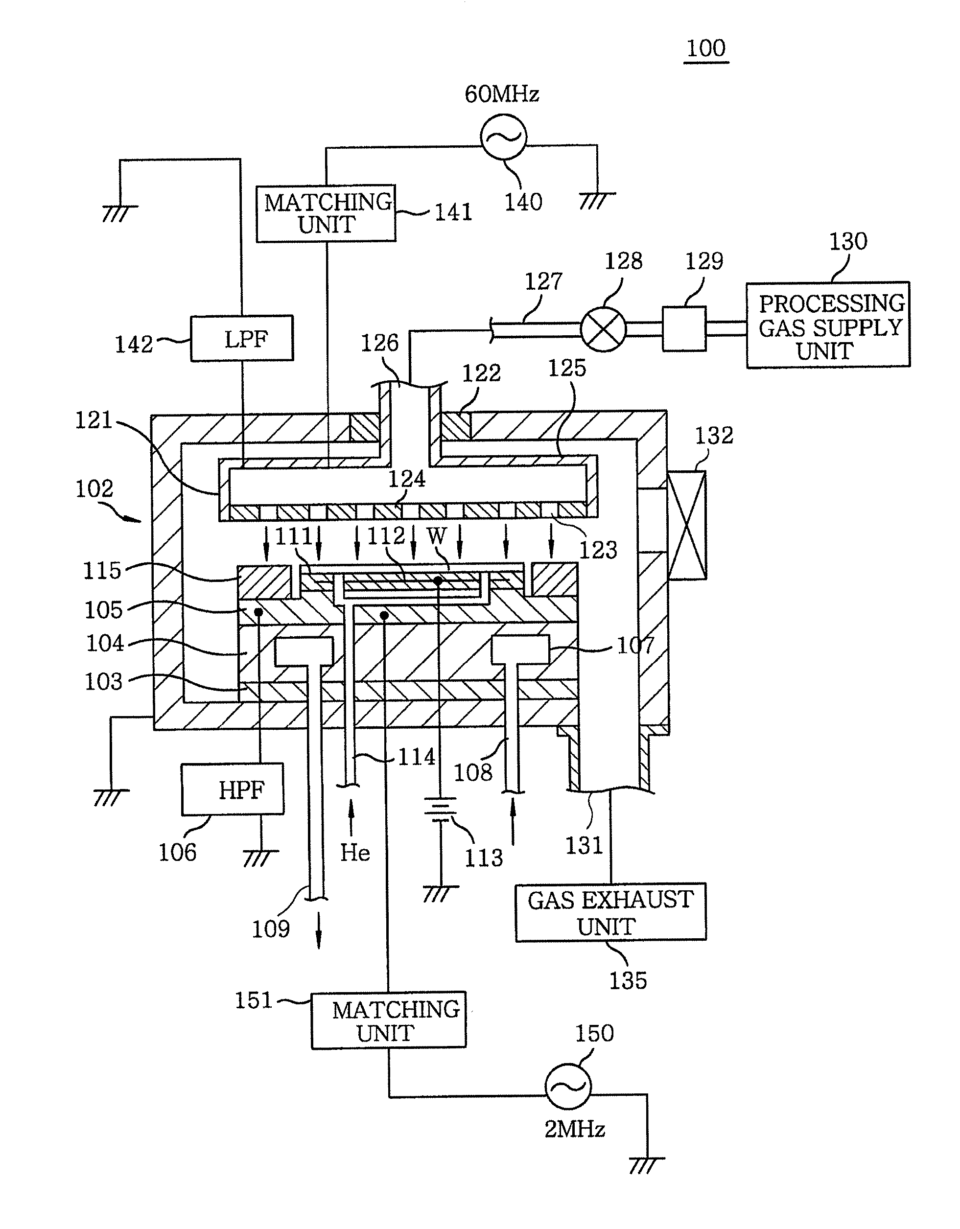
[0048] The schematic construction of plasma processing apparatus according to a first embodiment of the present invention is described with reference to the drawings. FIG. 1 is a sectional view illustrating an example of the construction of the plasma processing apparatus according to the first embodiment. Here, a parallel plate-type plasma etching apparatus is taken as an example of the plasma processing apparatus.

[0049] A plasma processing apparatus 100 includes a processing chamber 102 that has a processing container, the surface of which is made of aluminum having been subjected to, for example, an anode oxidization process (an alumite process), and which is formed in a cylindrical shape. The processing chamber 102 is grounded. A susceptor support 104 having an approximately cylindrical shape is provided on a bottom of the processing chamber 102. The susceptor support 104 mount a wafer W thereon, with an insulating plate 103 made of ceramic being interposed therebetween. A susc...

second embodiment

[0122] A second embodiment of the present invention is described below with reference to the drawings. Since the constructions of the plasma processing apparatus 100 and the optical measuring instrument 200 used in the second embodiment are the same as those illustrated in FIGS. 1 and 2, a detailed description thereof is omitted here. In the second embodiment, a description is made below, taking as an example the case where wafer types are classified according to the type of mask pattern formed on the film to be etched and an optimal end point detection recipe (for example, film thickness data) is used according to the type of mask pattern.

[0123] (Wafer Type and End Point Detection Setting Data)

[0124] There is a case where an accurate etching end point cannot be detected depending on the type of mask pattern. In the second embodiment, types of wafers having different types of mask patterns are determined, and the end point detection method according to the type of each mask patter...

third embodiment

[0138] A third embodiment of the present invention is described below with reference to the drawings. Since the constructions of the plasma processing apparatus 100 and the optical measuring instrument 200 according to the third embodiment are the same as those illustrated in FIGS. 1 and 2, detailed descriptions thereof are omitted here. In the third embodiment, a description is made, taking as an example the case where wafer types are classified according to the type of material of the mask formed on a film to be etched and an optimal end point detection method is used according to the type of material of the mask.

[0139] (Wafer Type and End Point Detection Setting Data)

[0140] There is a case where the end point of etching cannot be accurately detected due to the different types of material of the mask (for example, a hard mask and a photoresist mask) Accordingly, in the third embodiment, the types of wafers are determined based on the type of mask material, and an end point detec...


PUM

PropertyMeasurementUnit
Thicknessaaaaaaaaaa
Ratioaaaaaaaaaa
Optical propertiesaaaaaaaaaa

Abstract

In a plasma processing method, a correlation between substrate type data and optical data is obtained by using a multivariate analysis; substrate type data is obtained from optical data based on the correlation when initiating a plasma processing; and a substrate type is determined by using the obtained substrate type data. Further, a setting data set corresponding to the determined substrate type is selected from setting data sets, each for detecting a plasma processing end point of the plasma processing, each of the setting data sets being stored in advance in a data storage unit; an end point of the plasma processing is detected based on the selected setting data set; and the plasma processing is terminated at the detected end point.

Description

FIELD OF THE INVENTION [0001] The present invention relates to plasma processing method and plasma processing apparatus for performing plasma processing on a substrate such as a semiconductor wafer or a liquid crystal substrate. BACKGROUND OF THE INVENTION [0002] Plasma processing of a substrate (for example, etching, film forming process, etc.) has been widely applied in semiconductor manufacturing processes and Liquid Crystal Display (LCD) substrate manufacturing processes. Plasma processing apparatus used for such plasma processing includes an upper electrode and a lower electrode disposed parallel to each other in a processing chamber, allows a substrate, for example, a semiconductor wafer (hereinafter simply referred to as a “wafer”), to be mounted on the lower electrode, generates the plasma of processing gas by applying high-frequency power between the upper and lower electrodes, and etches a film using, for example, a patterned mask. [0003] In such plasma etching, the detect...

Claims


Application Information

Patent Timeline
IPC IPC(8): H01L21/66C23F1/00
CPCH01J37/32935H01L22/26H01J37/32963
Inventor OGASAWARA, KOSUKESAITO, SUSUMUNOZAWA, SYUJI
Owner TOKYO ELECTRON LTD
Why Eureka
Try Eureka