Silicon carbide single crystals with low boron content

a technology of silicon carbide and single crystals, which is applied in the direction of single crystal growth details, single crystal growth, chemistry apparatus and processes, etc., can solve the problems of contaminating the growing crystal and the loss of silicon from the growth charge, so as to reduce the chemical attack on the sic source and reduce the loss. , the effect of reducing the loss

Active Publication Date: 2008-03-27
II VI DELAWARE INC
View PDF9 Cites 54 Cited by
  • Summary
  • Abstract
  • Description
  • Claims
  • Application Information

AI Technical Summary

Benefits of technology

[0021] Lower halosilanes can attack the SiC source and growing crystal, leading to losses of silicon from the growth charge. In order to reduce these losses, the gas mixture can include small amounts of hy

Problems solved by technology

Generally, graphite contains detectable levels of boron impurity, which can contaminate the growing crystal.
Lowe

Method used


Image

  • Silicon carbide single crystals with low boron content
  • Silicon carbide single crystals with low boron content
  • Silicon carbide single crystals with low boron content

Examples


Embodiment Construction

[0040] The following embodiment will be described with reference to the accompanying figures where like reference numbers correspond to like elements.

[0041] SiC sublimation growth is conducted under a dynamic reactive atmosphere containing halogen. Halogen converts boron, whether free or chemically bound, into volatile boron halides that are removed from the interior of the growth crucible by the flow of inert carrier gas filtering across the permeable crucible wall.

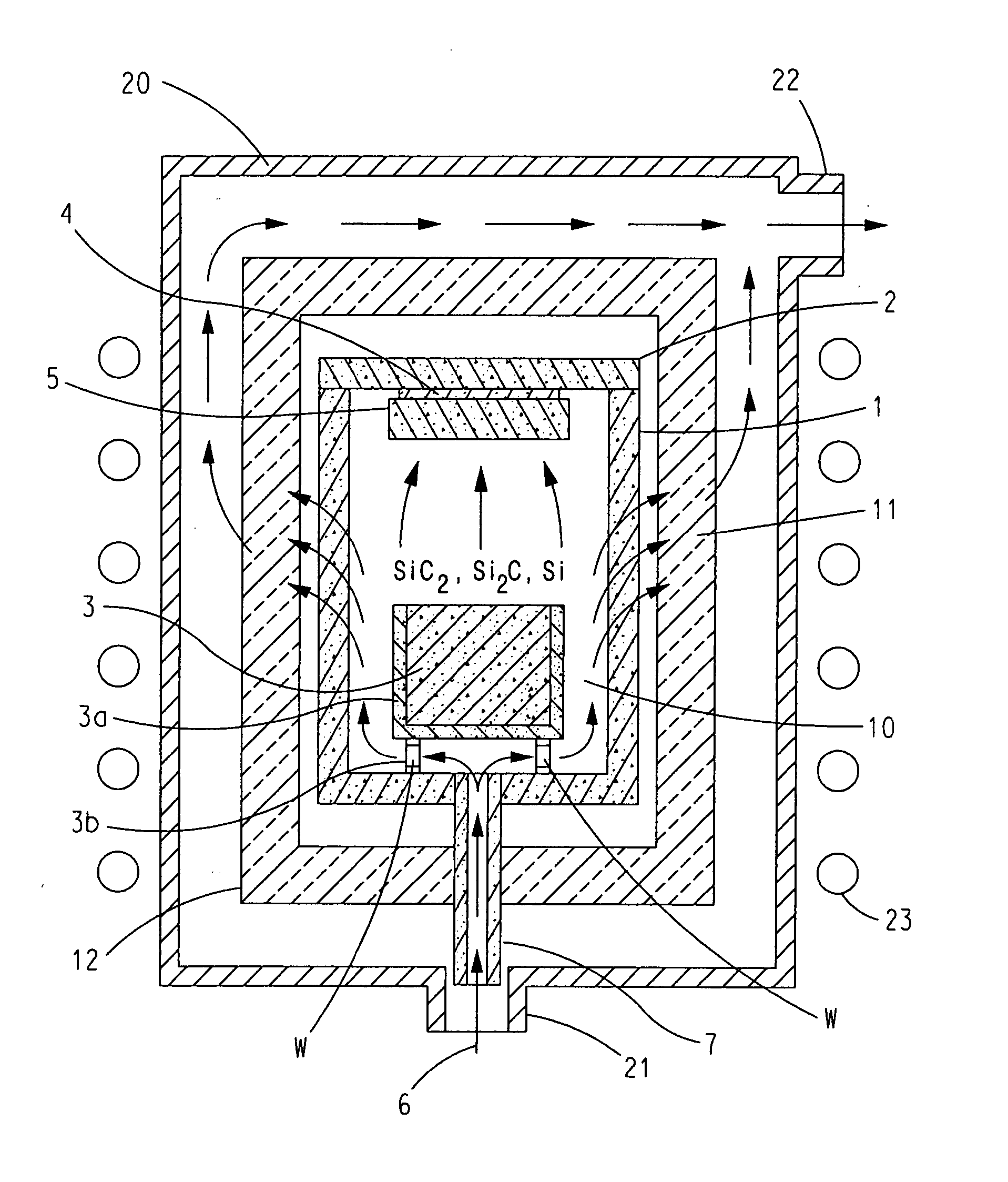
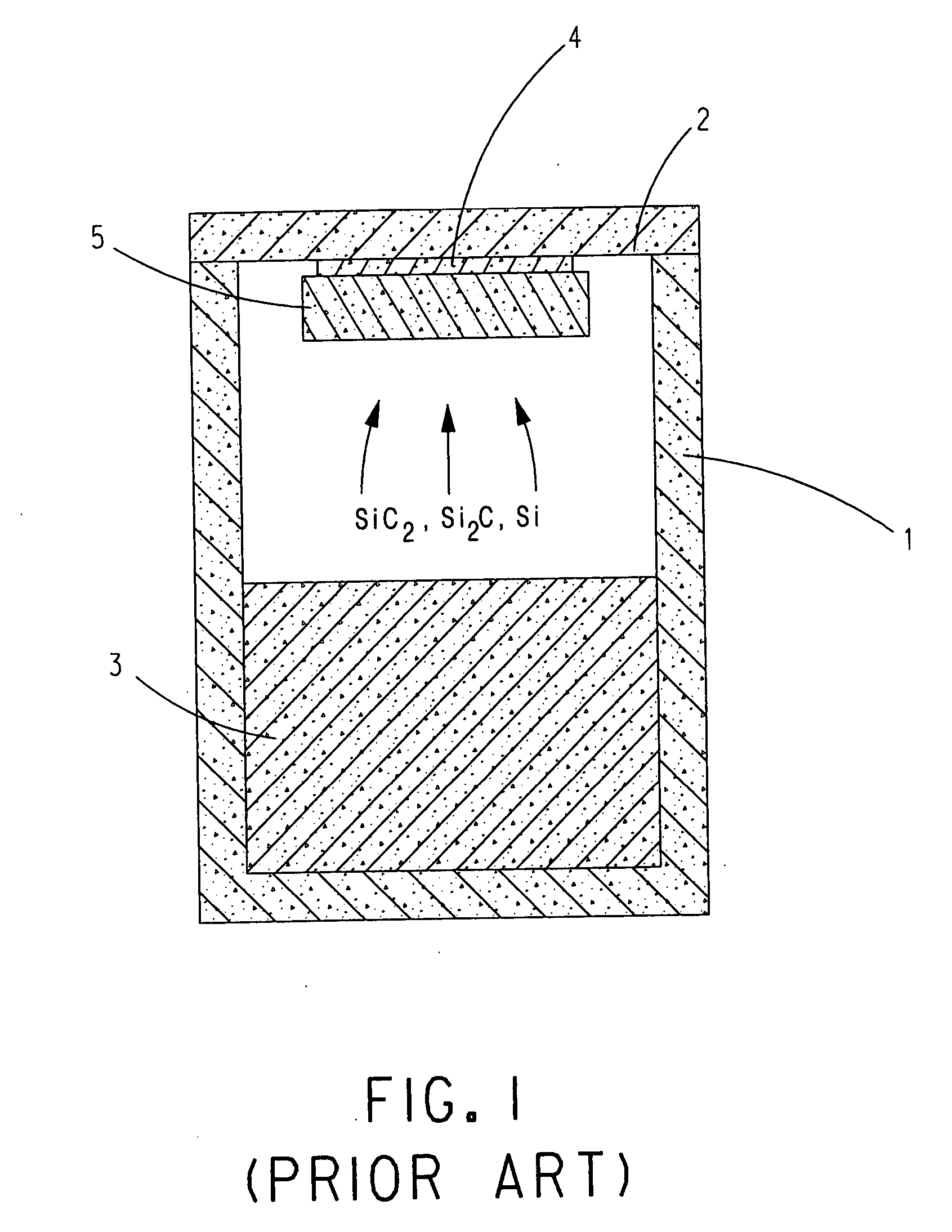
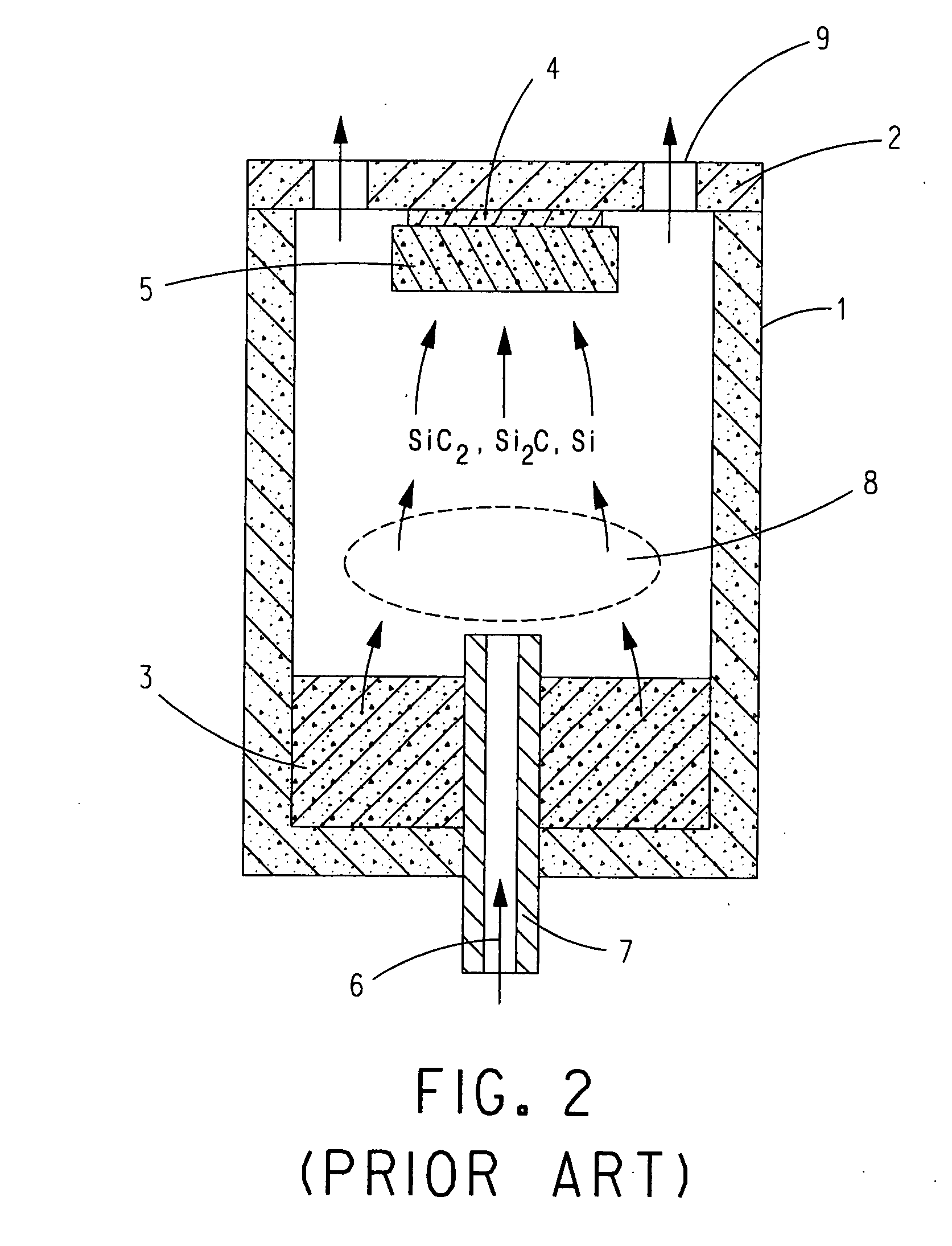
[0042] With reference to FIG. 3, more specifically, PVT sublimation growth of silicon carbide is carried out in a graphite growth crucible 1 sealed with a graphite lid 2. Desirably, crucible 1 and lid 2 are made of high-density, fine-grain and low-porosity graphite, such as “ATJ” available from Union Carbide Corporation of Danbury, Conn., under registered trademark UCAR® (registration number 1008278), or similar. Growth crucible 1 is loaded with a SiC polycrystalline source 3 and a noncrystalline seed crystal 4. Source...


PUM


Abstract

In a crystal growth method, an enclosed growth crucible is provided inside of a growth chamber. The growth crucible has polycrystalline source material and a seed crystal disposed in spaced relation therein. The interior of the growth crucible is heated whereupon a temperature gradient forms between the source material and the seed crystal. The temperature gradient is sufficient to cause the source material to sublimate and be transported to the seed crystal where it precipitates on the seed crystal. A gas mixture is caused to flow into the growth crucible and between the polycrystalline source material and an interior surface of the growth crucible. The gas mixture reacts with an unwanted element in the body of the growth crucible to form a gaseous byproduct which then flows through the body of the growth crucible to the exterior of the growth crucible.

Description

CROSS REFERENCE TO RELATED APPLICATIONS [0001] This application claims priority from U.S. provisional patent application No. 60 / 847,318, filed on Sep. 26, 2006, and is a continuation-in-part of U.S. patent application Ser. No. 11 / 784,971, filed Apr. 10, 2007, the contents of both of which are incorporated herein by reference.BACKGROUND OF THE INVENTION [0002] 1. Field of the Invention [0003] The present invention relates to the growth of SiC crystals having a reduced boron content. [0004] 2. Description of Related Art [0005] Wafers of semi-insulating silicon carbide of 4H and 6H polytypes serve as lattice-matched substrates to grow epitaxial layers of SiC and AlGaN, which are used for the fabrication of SiC- and AlGaN-based microwave devices. In order for the devices to work efficiently, the substrates must be semi-insulating, that is, fully compensated electronically. In practical terms, it is required that the resistivity of the SiC substrate must be higher than 105 Ohm·cm, and de...

Claims


Application Information

Patent Timeline
IPC IPC(8): C30B29/10C30B25/00
CPCC30B29/36C30B23/00
Inventor ZWIEBACK, ILYAANDERSON, THOMAS E.GUPTA, AVINASH K.
Owner II VI DELAWARE INC
Why Eureka
Try Eureka