Back contact device for photovoltaic cells and method of manufacturing a back contact device

a photovoltaic cell and back contact technology, applied in the field of photovoltaic cells, can solve the problems of high cost of producing cells and pv modules, lack of widespread use of pv cells as a source of electricity, and the addition of high purity wafers to the process of manufacturing pv cells and modules, and achieve the effect of increasing the crystallinity of the semiconductor layer

Inactive Publication Date: 2008-03-27
THINSILICION CORP
View PDF103 Cites 83 Cited by
  • Summary
  • Abstract
  • Description
  • Claims
  • Application Information

AI Technical Summary

Benefits of technology

[0022]One or more embodiments of the presently described invention provides a method for fabricating an all-back contact photovoltaic cell. The method includes the steps of depositing a semiconductor layer on a non-opaque substrate, increasing a level of crystallinity of the semiconductor layer by exposing it to a focused beam of energy, doping the semiconductor layer with first and second dopants on one side to create at least two doped regions, and providing electrical contacts to the doped regions by depositing a conductive layer on the semiconductor layer so that the electrical contacts are on the same side of the semiconductor layer while incident light strikes the layer from an opposing side.

Problems solved by technology

One key factor contributing to the lack of widespread usage of PV cells as a source of electricity is the cost of producing the cells and PV modules.
Producing or purchasing such high purity wafers adds significant expense to the process of manufacturing PV cells and modules.
As the thickness of semiconductor materials in PV cells increases above this range, the extra semiconductor material contributes only marginally to light absorption in the PV cell, so the cell efficiency does not increase substantially.
Therefore, while semiconductor wafers must usually be made 150 to 300 μm, or 150×10−6 to 300×10−6 m, thick for mechanical handling purposes, a significant fraction of the thickness of the wafer can be effectively useless from the standpoint of increasing the efficiency of the cell.
The cost of producing a thin semiconductor film on a low-cost carrier substrate typically is significantly less than manufacturing or obtaining an electronic-grade semiconductor wafer.
While the use of a thin semiconductor film instead of an electronic-grade semiconductor wafer can lower the cost of a PV cell while maintaining the same efficiency, an additional challenge is the deposition of the semiconductor film.
In order to produce a crystalline or polycrystalline thin semiconductor film, expensive and time-consuming deposition techniques must be used.
In addition, the polysilicon PECVD technique usually yields very little control over the film morphology and grain size, with a typical grain size in the 1 to 50 nm, or 1×10⁻⁹ to 50×10−9 m, range.
However, typically the processing temperature for crystallizing the films is often outside the temperature range that can be withstood for a long duration of time by low-cost carrier substrates because the temperature can exceed the softening point of the substrates.
Thus, making electrical contact to semiconductor films that are crystallized (or at least have their crystallinity increased) using ZMR remains a challenge.
Achieving a minority carrier diffusion length in the range 500 μm to 1 millimeter (“mm”), or 500×10−6 to 1×10⁻³ m (as can be necessary in the case of thick, wafer-based cells) requires very pure and nearly structurally perfect silicon, resulting in a significant increase in the cost of the wafers.
Thus, there is a smaller area for incident light to strike the semiconductor material and the efficiency of these designs decreases.
An additional problem with existing methods of manufacturing PV cells and with existing ZMR techniques is the speed at which the semiconductor films are crystallized or have their level of crystallinity increased.
For example, in crystallizing semiconductor films using e-beams, existing e-beam systems cannot uniformly cover or expose a large-area substrate, such as a substrate that is greater than 1 m2.
In addition, while large-area scanning methods have been devised in electron beam curing systems, this has not yet been accomplished in systems involving highly focused line-source e-beams in a vacuum environment.
While existing methods can generate a small-length focused line-source e-beam for processing semiconductor films, the length of the e-beam line is limited.
For example, some existing methods can only produce e-beam lines with lengths on the order of 2 to 10 centimeters (“cm”).
However, the length of the emitted e-beam line is limited.
However, the position of the filament is very difficult to control over increasing distances because the position of the filament must be accurate to within a fraction of a millimeter over its length.
Thus, adjusting the position of the filament can be an impractical solution for beam lengths above 10 cm.
In addition, it can be very difficult to maintain the precise geometry of a Pierce reflector system over the width of a large-area substrate, which may be as wide as 2 to 3 m across.
These factors make it very difficult (if not impossible) to obtain a uniform crystallization pattern over large-area substrates using a line e-beam generated from a single filament.
However, the substrate area that can be covered using a point source e-beam in existing systems and methods is also limited, as evidenced by the very large aspect ratios, undesirable screen curvature, and limited screen size of state-of-the-art cathode ray tubes.

Method used


Image

  • Back contact device for photovoltaic cells and method of manufacturing a back contact device
  • Back contact device for photovoltaic cells and method of manufacturing a back contact device
  • Back contact device for photovoltaic cells and method of manufacturing a back contact device

Examples


Embodiment Construction

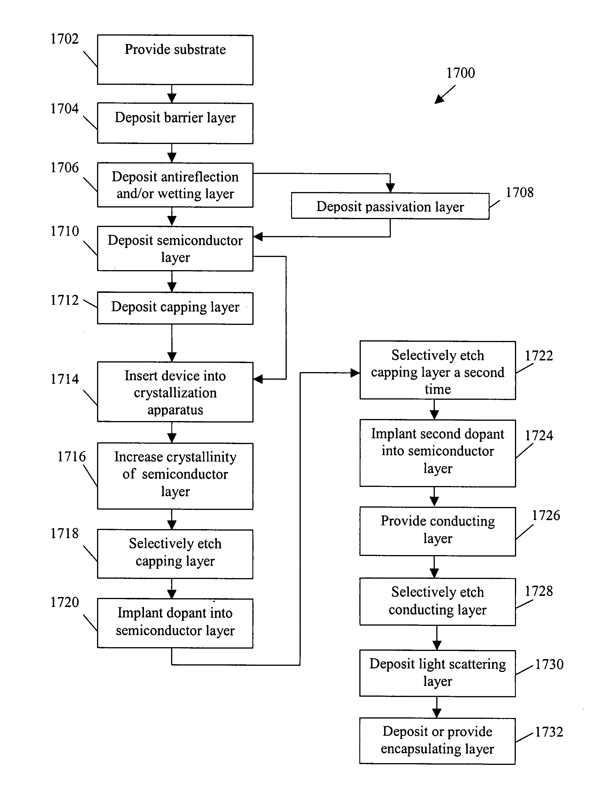
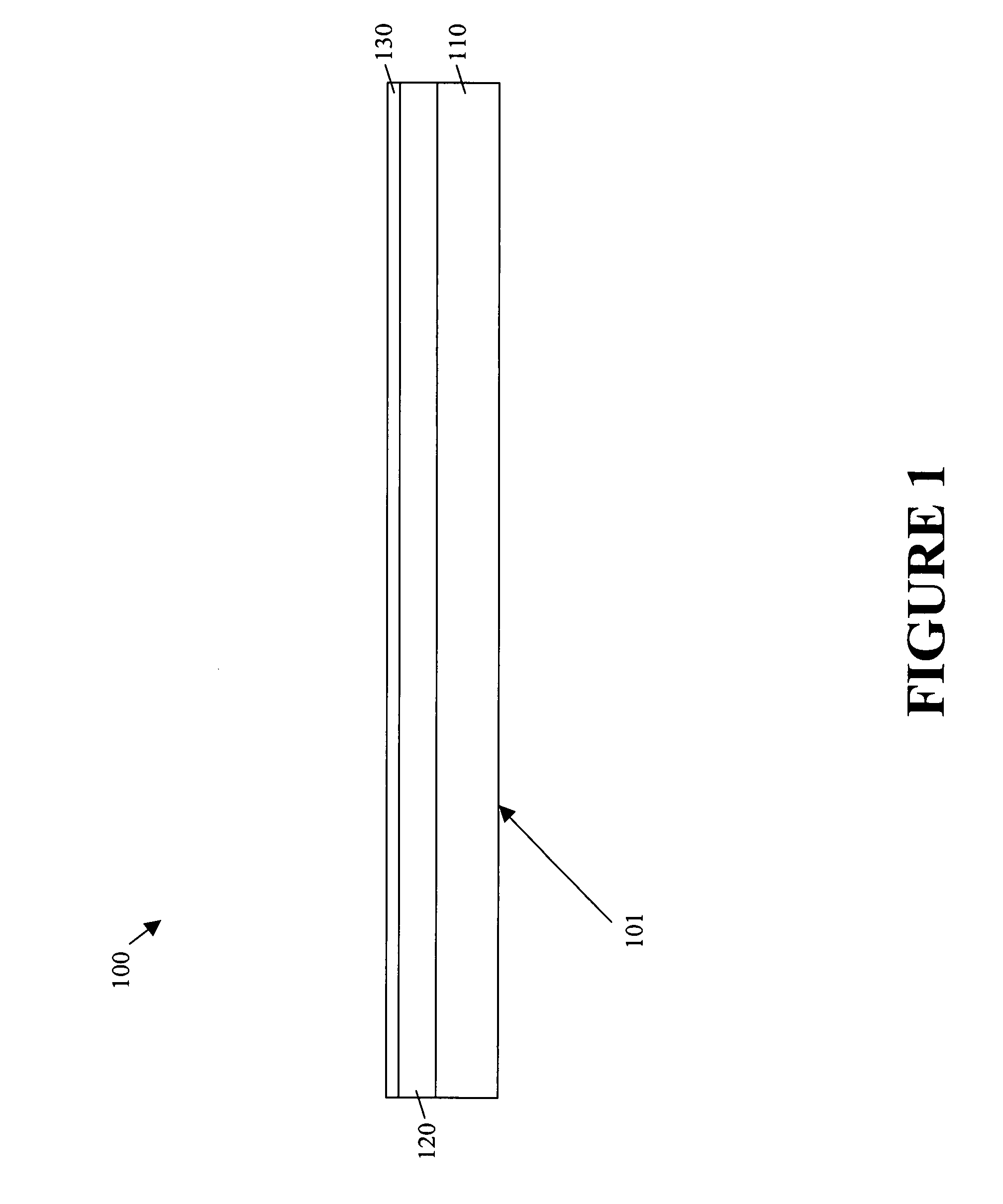
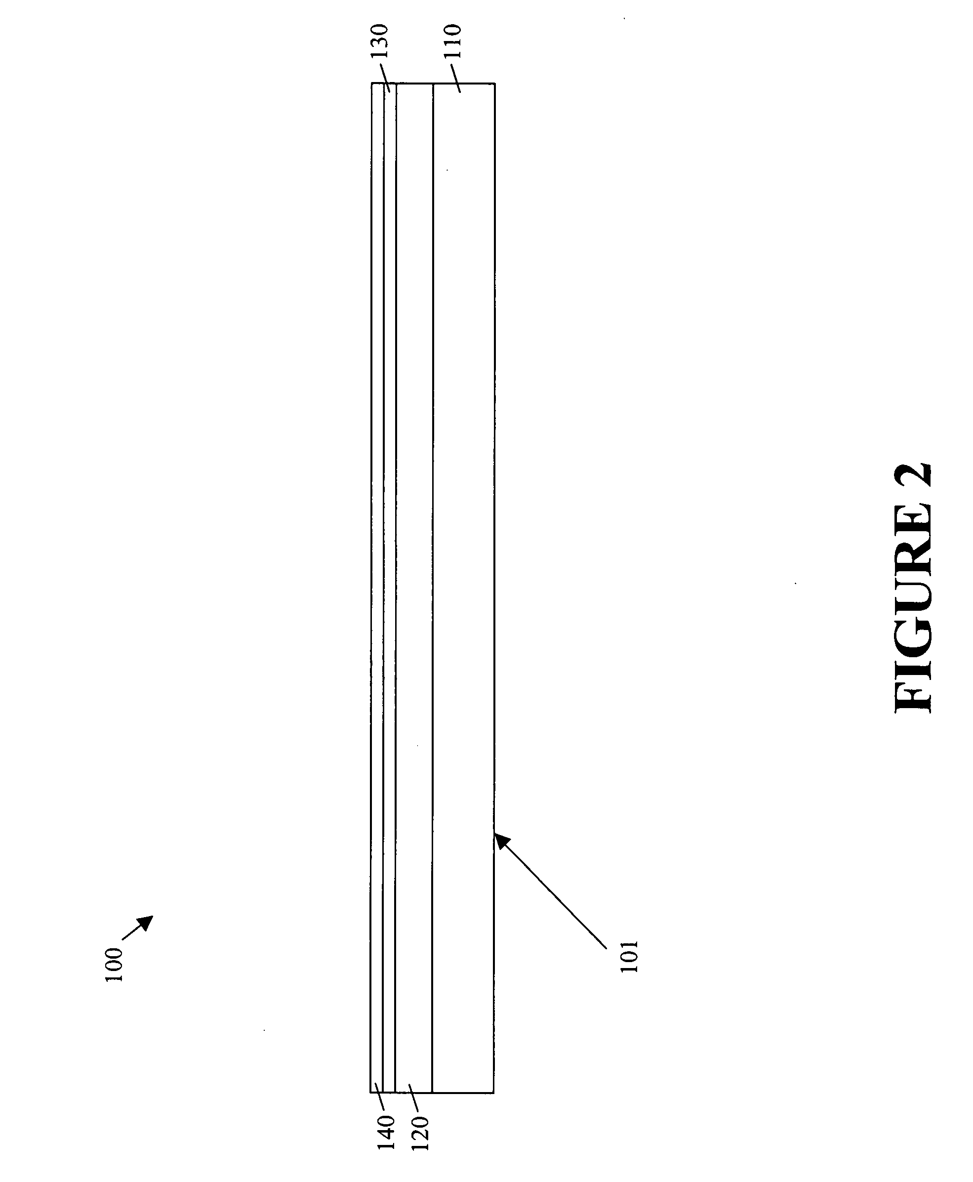
[0048]FIG. 17 illustrates a flowchart of a method 1700 for fabricating an all-back contact thin film PV cell in accordance with an embodiment of the presently described invention. Various steps illustrated in FIG. 17 and described herein are illustrated in other figures. For example, FIGS. 1-16 illustrate a cross-section view of a PV cell 100 fabricated in accordance with an embodiment of the presently described invention at one or more of the steps illustrated and described in FIG. 17. In general, cell 100 includes a side 101 that incident light strikes to generate electricity. For example, light incident to cell 100 at side 101 passes through one or more layers of cell 100 (including a substrate 110, as described below) and strikes a semiconductor layer 155 (also described below) to generate electricity.

[0049]In accordance with an embodiment of method 1700 and as illustrated in FIG. 1, a substrate 110 is first provided or obtained at step 1702. Substrate 110 preferably comprises a...


PUM


Abstract

One or more embodiments of the presently described invention provide a method for fabricating an all-back contact photovoltaic cell. The method includes the steps of depositing a semiconductor layer on a non-opaque substrate, increasing a level of crystallinity of the semiconductor layer by exposing it to a focused beam of energy, doping the semiconductor layer with first and second dopants on one side to create at least two doped regions, and providing electrical contacts to the doped regions by depositing a conductive layer on the semiconductor layer so that the electrical contacts are on the same side of the semiconductor layer while incident light strikes the layer from an opposing side.

Description

CROSS-REFERENCE TO RELATED APPLICATIONS[0001]This application is a nonprovisional utility application that claims priority benefit of copending U.S. Provisional Patent application Ser. Nos. 60 / 932,374 (the “'374 application”), 60 / 932,389 (the “'389 application”), 60 / 932,395 (the “'395 application”) and 60 / 847,475 (the “'475 application). The '374 application was filed on May 31, 2007, and is entitled “Method of Annealing a Large Area Semiconductor Film Using Electron Beams.” The '389 application was filed on May 31, 2007, and is entitled “Method of Producing a Microcrystalline Silicon Film for Photovoltaic Cells.” The '395 application was filed on May 31, 2007, and is entitled “Method of Producing a Photovoltaic Module.” The '475 application was filed on Sep. 27, 2006, and is entitled “Back Contact Device for Photovoltaic Cells.” The entire disclosures of the '375, '389, '395 and '475 applications are incorporated by reference herein in their entirety.BACKGROUND OF THE INVENTION[000...

Claims


Application Information

Patent Timeline
Patent Type & Authority Applications(United States)
IPC IPC(8): H01L31/042
CPCY02E10/52H01L31/022441Y02E10/547H01L31/0682H01L31/1804H01L31/0516Y02P70/50
Inventor STEPHENS, JASON M.COAKLEY, KEVIN MICHAELHUSSEN, GULEID
Owner THINSILICION CORP
Why Eureka
Try Eureka